Monocrystal FBAR piezoelectric film and preparation method thereof

A piezoelectric film and crystal piezoelectric technology, applied in the direction of electrical components, impedance networks, etc., can solve problems such as damage to single crystal piezoelectric film, damage to single crystal piezoelectric film, and incomplete decomposition of the peeling layer to achieve high-quality factors Good, improve the accuracy, save the effect of the process

Pending Publication Date: 2022-04-15
ZHEJIANG UNIV HANGZHOU GLOBAL SCI & TECH INNOVATION CENT
View PDF0 Cites 1 Cited by
  • Summary
  • Abstract
  • Description
  • Claims
  • Application Information

AI Technical Summary

Problems solved by technology

However, the peeling layer will not be completely decomposed, and the remaining peeling layer needs to be removed. In the prior art, it is inevitable to damage the single crystal piezoelectric film during the process of removing the remaining peeling layer. In addition, due to the substrate used in the prior art and the grown Thin film, e.g.: ALN piezoelectric film, SiO 2 The bonding layer is a transparent layer, which poses certain challenges to using mature optical film thickness meter technology to accurately test the thickness of the piezoelectric film in different regions online
[0008] Therefore, it is urgent to solve the technical problems that the peeling layer removal process will damage the single crystal piezoelectric film, thereby affecting the uniformity of the piezoelectric film surface of the single crystal FBAR, and the thickness of the single crystal piezoelectric film in different regions cannot be accurately measured, thus affecting The subsequent trimming process directly affects the yield of the device

Method used


Image

  • Monocrystal FBAR piezoelectric film and preparation method thereof
  • Monocrystal FBAR piezoelectric film and preparation method thereof
  • Monocrystal FBAR piezoelectric film and preparation method thereof

Examples


Embodiment 1

[0087]The present invention also provides a method for preparing a cavity type thin film bulk acoustic resonator, the specific steps are as follows:

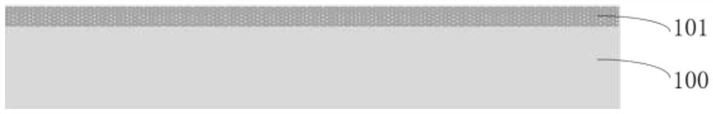
[0088] (1) Cleaning the double-polished sapphire substrate 100, using acetone and isopropanol for ultrasonic washing, and the orientation of the sapphire substrate is C(0001);

[0089] (2) if figure 1 As shown, a GaN film of 1 μm is deposited on the surface of the double-polished sapphire substrate 100 by magnetron sputtering or MOCVD as the lift-off layer 101. The growth process of the GaN film: the TMGa gas flow rate is 20 sccm, the NH 3 The gas flow rate is 800sccm, the growth temperature is 1000°C, the chamber pressure is 30mbar, and the growth rate is about 10nm / min. Sometimes, in order to make the GaN film more compatible with the sapphire substrate, a layer of about 100nm is sputtered before growing the GaN film. ALN film;

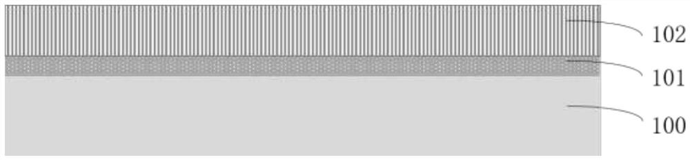
[0090] (3) if figure 2 As shown, a 800nm ​​ALN single crystal piezoelectric film 102 is deposi...


PUM

PropertyMeasurementUnit
thicknessaaaaaaaaaa
depthaaaaaaaaaa
widthaaaaaaaaaa

Abstract

The invention discloses a cavity film bulk acoustic resonator which comprises a first substrate, a bonding layer, an opaque dielectric layer, a piezoelectric oscillation pile and a metal pad layer. Wherein a bonding layer is formed on the first substrate, an opaque dielectric layer is formed on the bonding layer, a piezoelectric oscillation pile is formed on the opaque dielectric layer, a cavity is formed between the opaque dielectric layer and the piezoelectric oscillation pile, and the metal pad layer is connected with the piezoelectric oscillation pile. The surface roughness of the resonator is low, and the thickness of each area of the film can be measured conveniently and accurately. The invention also discloses a preparation method of the cavity film bulk acoustic wave resonator, and the preparation method saves preparation processes, and is simple and efficient.

Description

technical field [0001] The invention belongs to the technical field of semiconductors, and in particular relates to a single crystal FBAR piezoelectric thin film and a preparation method thereof. Background technique [0002] With the rapid development of mobile communication technology, the market demand for high frequency band resonators and filters is increasing. Compared with traditional microwave ceramic resonators and surface acoustic wave resonators, film bulk acoustic resonators (FBARs) have the advantages of small size, low loss, high quality factor, large power capacity, and high resonance frequency, so they are especially popular in related fields. It has a broad application prospect in high-frequency communication, and has become a research hotspot in the industry and academia. [0003] The filter performance level is determined by its high-quality factor (Factor of merit), which is defined as FOM=Q*K 2 eff, where Q is the quality factor, which describes the vi...

Claims


Application Information

Patent Timeline
Patent Type & Authority Applications(China)
IPC IPC(8): H03H3/02H03H9/17
Inventor 董树荣轩伟鹏刘刚金浩高峰骆季奎
Owner ZHEJIANG UNIV HANGZHOU GLOBAL SCI & TECH INNOVATION CENT
Why Eureka
Try Eureka