
Formation method of semiconductor structure and semiconductor structure

A semiconductor and contact structure technology, which is applied in semiconductor/solid-state device manufacturing, transistors, electrical components, etc., and can solve problems such as short-circuiting of wires in capacitive contact pads and partial structural damage of virtual capacitive contact structures.

Pending Publication Date: 2022-04-29
CHANGXIN MEMORY TECH INC
View PDF0 Cites 3 Cited by
  • Summary
  • Abstract
  • Description
  • Claims
  • Application Information

AI Technical Summary

Problems solved by technology

[0004] In the DRAM manufacturing process, the dummy capacitive contact structure and the dummy bit line structure are the most common dummy structures. However, the applicant found that due to the requirements of the manufacturing process, multiple wet cleaning processes are required in the process flow of the capacitive contact structure. , leading to the destruction of part of the structure of the virtual capacitive contact structure, thereby forming a deep cavity. With the shrinking of the critical size, the wiring of the capacitive contact pad becomes denser and denser. Filled with metal material, resulting in a short circuit of the wires of the formed capacitive contact pads

Method used


Image

  • Formation method of semiconductor structure and semiconductor structure
  • Formation method of semiconductor structure and semiconductor structure
  • Formation method of semiconductor structure and semiconductor structure

Examples


Embodiment Construction

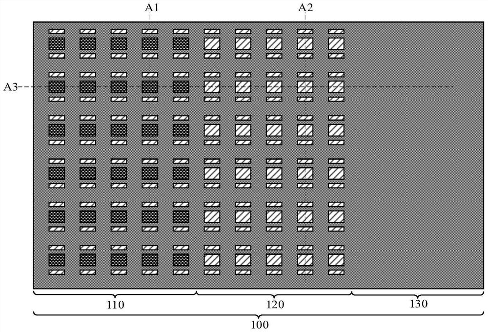
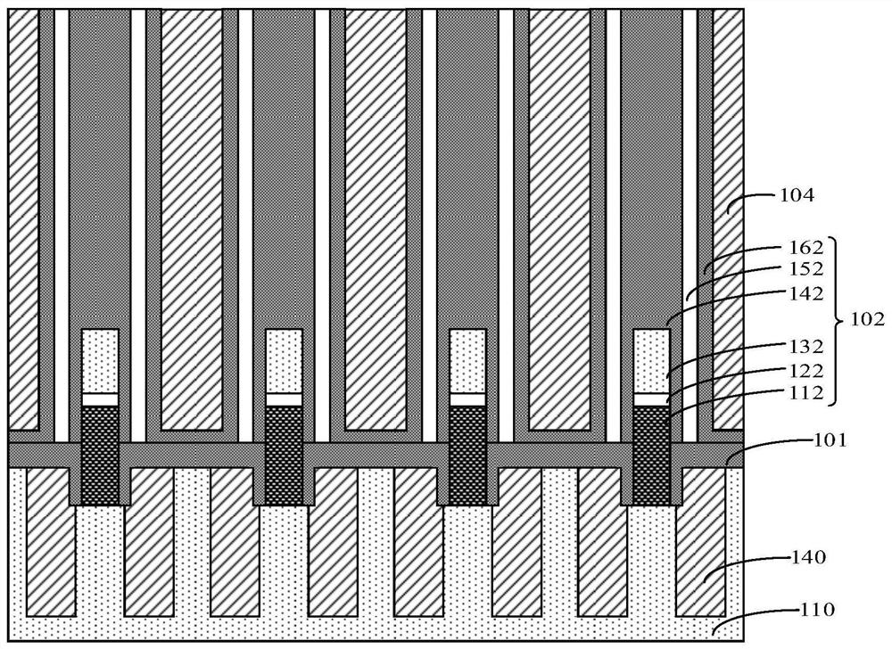
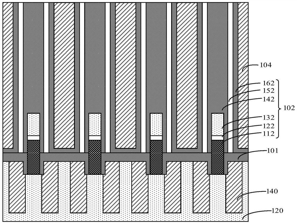
[0026] At present, due to the requirements of the manufacturing process, multiple wet cleaning processes are required in the process flow of the capacitive contact structure. The wet cleaning process has an etching load effect, and the etching rate of the etch-intensive area will be correspondingly reduced. , resulting in over-etching of other structures during the process of forming the capacitive contact opening, for example, over-etching of the dummy capacitive contact structure, resulting in deep voids in the dummy capacitive contact structure. Later, when forming the wires of the capacitor contact pads, some metal materials are filled into the cavities. With the shrinking of the key dimensions, the wires of the capacitor contact pads are arranged more and more densely, and the conductive part of the metal materials of the adjacent capacitor contact pads may be filled. into the same void, resulting in short circuiting of the wires of the formed capacitive contact pad.

[0...


PUM


Abstract

The embodiment of the invention provides a forming method of a semiconductor structure and the semiconductor structure, and the method comprises the steps: providing a substrate which comprises a contact region and a virtual region which are adjacently arranged, and forming a bit line structure and a dielectric layer which are separately arranged on the substrate, the extension direction of the dielectric layer intersects with the extension direction of the bit line structure, and the bit line structure and the dielectric layer enclose an erected capacitor contact opening; forming a sacrificial layer filling the capacitor contact opening; removing the sacrificial layer in the contact region to form a second opening; forming a bottom conductive layer filling the second opening; in the virtual region, removing partial height of the sacrificial layer to form a first opening; forming an insulating layer filling the first opening; according to the embodiment of the invention, the problem of wire short circuit of the capacitor contact pad along with the reduction of the critical dimension is avoided.

Description

technical field [0001] The invention relates to the field of semiconductors, in particular to a method for forming a semiconductor structure and the semiconductor structure. Background technique [0002] The development of Dynamic Random Access Memory (DRAM) pursues the performance characteristics of high speed, high integration density and low power consumption. [0003] With the shrinking of the semiconductor structure size, especially in the DRAM manufacturing process with a critical dimension less than 20nm, the etching load effect of the DRAM array area and the peripheral area is increasing. In order to ensure the integrity and effectiveness of the circuit structure of the DRAM array area, It is usually necessary to design virtual structures in the array area. [0004] In the DRAM manufacturing process, the dummy capacitive contact structure and the dummy bit line structure are the most common dummy structures. However, the applicant found that due to the requirements ...

Claims


Application Information

Patent Timeline
IPC IPC(8): H01L21/8242H01L27/108
CPCH10B12/03H10B12/30H10B12/09H10B12/00
Inventor 陈龙阳武宏发吴公一
Owner CHANGXIN MEMORY TECH INC
Learn More