Supercharge Your Innovation With Domain-Expert AI Agents!

Variable-grid core particle arrangement optimization algorithm

An optimization algorithm and grid technology, applied to the photoplate-making process of the pattern surface, microlithography exposure equipment, instruments, etc., can solve the problems of inaccurate results, large amount of calculation, time-consuming and other problems, and achieve the goal of overcoming the problem of seeking Optimize the effect of large amount of calculation, ensure accuracy, and shorten calculation time

Pending Publication Date: 2022-05-06
SIEN QINGDAO INTEGRATED CIRCUITS CO LTD
View PDF0 Cites 0 Cited by
  • Summary
  • Abstract
  • Description
  • Claims
  • Application Information

AI Technical Summary

Problems solved by technology

[0006] In view of the above-mentioned shortcomings of the prior art, the purpose of the present invention is to provide a variable grid core grain arrangement optimization algorithm, which is used to solve the large amount of calculation and inaccurate results existing in the existing fixed grid optimization algorithm. , time-consuming and other issues

Method used


Image

  • Variable-grid core particle arrangement optimization algorithm
  • Variable-grid core particle arrangement optimization algorithm
  • Variable-grid core particle arrangement optimization algorithm

Examples


Embodiment 1

[0041] This embodiment provides a Die arrangement optimization algorithm with variable grid, specifically as follows:

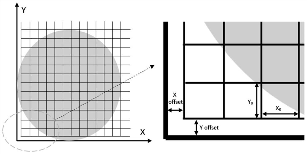
[0042] S1: Establish a rectangular coordinate system, the X and Y axes of the rectangular coordinate system are tangent to the edge of the wafer.

[0043] S2: Taking the origin of the coordinates as the starting point, using the dichotomy method to find the optimal combination of offsets X offset and Y offset, so that the number of Dies divided on the wafer is the largest, and an array arrangement of Dies is obtained.

[0044] The step S2 specifically includes the following steps:

[0045] S2-1: Die length and width X 0 , Y 0 Divide them into 10 equal parts, and the length and width of each part are X 0 / 10, Y 0 / 10;

[0046] S2-2: Set the X-direction offset X offset of Die arrangement to X in turn 0 / 10, 2X 0 / 10,...,X 0 ;Set the Y-direction offset Y offset of Die arrangement to Y in sequence 0 / 10, 2Y 0 / 10,...,Y 0 . A total of 10*10=100 combina...

Embodiment 2

[0051] This embodiment also provides a calculation method for the arrangement of Die arrays on a wafer, and the similarities with Embodiment 1 will not be repeated, and the difference lies in:

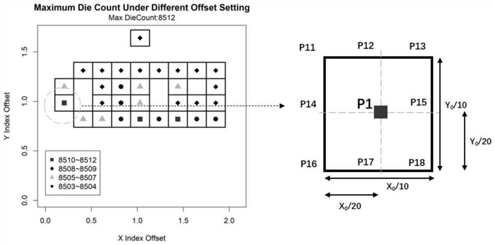
[0052] After finding the suspected points at all levels in Embodiment 1, cluster analysis is carried out to the suspected points at all levels respectively, as Image 6 As shown, the suspected points are classified, and each closed curve in the figure represents a class. The method of using cluster analysis to classify suspected points is as follows: calculate the spatial distance between each suspected point, set the threshold of the class, and classify the suspected points with the spatial distance smaller than this threshold and the corresponding Die Count value into one class. The threshold of the class is determined according to the series of suspected points. For example, the distance between the class I suspected points is far away, and the threshold of the class is relatively l...

Embodiment 3

[0056] This embodiment provides a method for calculating the Die array arrangement on a wafer. The method mainly performs Die array arrangement for wafers with unusable areas such as defects, flags, and engraved codes. The similarity with Embodiment 2 will not be described in detail, the difference is:

[0057] Before executing S2, it is necessary to divide the unusable area of ​​the wafer, such as Figure 9 As shown, these unusable areas are first accurately positioned on the wafer, and these areas are classified as invalid areas when performing array layout calculations, and these invalid areas are excluded when calculating Die Count, so that through the embodiment The optimal point obtained by the algorithm in 2 is the real optimal point, and it is also the most in line with the actual situation.


PUM


Abstract

The invention provides a variable-grid core particle arrangement optimization algorithm, which comprises the following steps of S1, establishing a rectangular coordinate system, and enabling an X axis and a Y axis of the rectangular coordinate system to be tangent to the edge of a wafer; s2, taking the origin of coordinates of the rectangular coordinate system as a starting point, and finding an optimal combination of offsets of the Die arrangement in the X direction and the Y direction by adopting a dichotomy, so that the number of the Dies divided on the wafer is maximum, and array arrangement of the Dies is obtained; s3, setting the X-direction offset and the Y-direction offset of a single exposure unit Shot according to the Die arrangement obtained in the S2, so that the number of Shots required for covering the wafer is minimum, and obtaining a Shot arrangement; according to the variable-grid core particle arrangement optimization algorithm provided by the invention, the calculation amount is far smaller than that of an existing fixed-grid optimization algorithm, the calculation time is greatly shortened, and meanwhile, result judgment is added to ensure the accuracy of a result. The method effectively overcomes the defects of large optimization calculation amount, long time consumption, inaccurate result and the like in the prior art, and has high practical value in the field of semiconductor manufacturing.

Description

technical field [0001] The invention relates to the field of semiconductor manufacturing, in particular to a core particle arrangement optimization algorithm with variable mesh. Background technique [0002] In the semiconductor manufacturing process, it usually involves the design of the die array arrangement on the entire wafer. The manufacturing cost of the wafer is expensive, so we need to divide as many Dies as possible on a fixed-size wafer. In the process of dividing the wafer, the photolithography process must be used. The complete photolithography process includes cleaning, gluing, soft baking, exposure, development, etching, detection and other processes, and exposure is to determine the final die. number of key steps. The exposure process is to transfer the pattern on the mask plate to the wafer, so the placement of the mask plate directly determines the final Die array arrangement, and the placement position of the mask plate is obtained through the prior Die ar...

Claims


Application Information

Patent Timeline
Patent Type & Authority Applications(China)
IPC IPC(8): G03F7/20
CPCG03F7/70491
Inventor 陈真林光启
Owner SIEN QINGDAO INTEGRATED CIRCUITS CO LTD
Features
  • R&D
  • Intellectual Property
  • Life Sciences
  • Materials
  • Tech Scout
  • Unparalleled Data Quality
  • Higher Quality Content
  • 60% Fewer Hallucinations
Learn More