Semiconductor structure and forming method thereof

A semiconductor and gate structure technology, which is applied in semiconductor devices, semiconductor/solid-state device manufacturing, semiconductor/solid-state device components, etc., can solve the problems of semiconductor structure damage, structural failure, and inability to protect metal gates well

Pending Publication Date: 2022-05-06
SEMICON MFG INT (SHANGHAI) CORP +1
View PDF0 Cites 0 Cited by
  • Summary
  • Abstract
  • Description
  • Claims
  • Application Information

AI Technical Summary

Problems solved by technology

[0003] However, if the metal gate is exposed for too long, grain defects may form, which in turn can easily lead to structural failure or even damage to the resulting semiconductor structure
[0004] In the prior art, the metal gate cannot be well protected, which eventually leads to poor performance of the device formed by the existing semiconductor process

Method used


Image

  • Semiconductor structure and forming method thereof
  • Semiconductor structure and forming method thereof
  • Semiconductor structure and forming method thereof

Examples


Embodiment Construction

[0047] It can be seen from the background art that the formation method of the semiconductor structure in the prior art is easy to cause damage to the gate structure, and the reason for the damage to the gate structure is analyzed in combination with a formation method of the semiconductor structure.

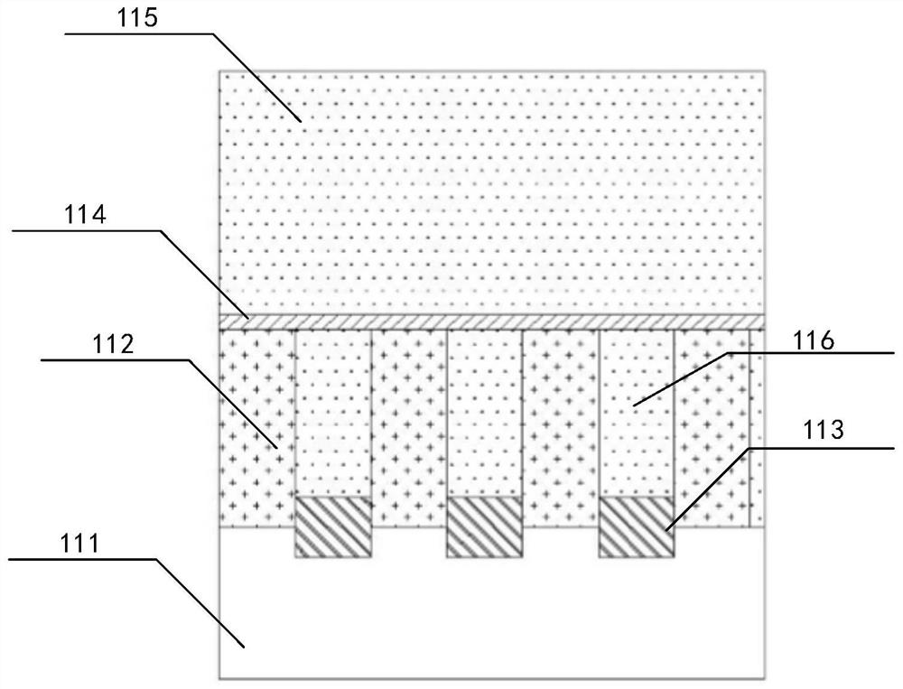
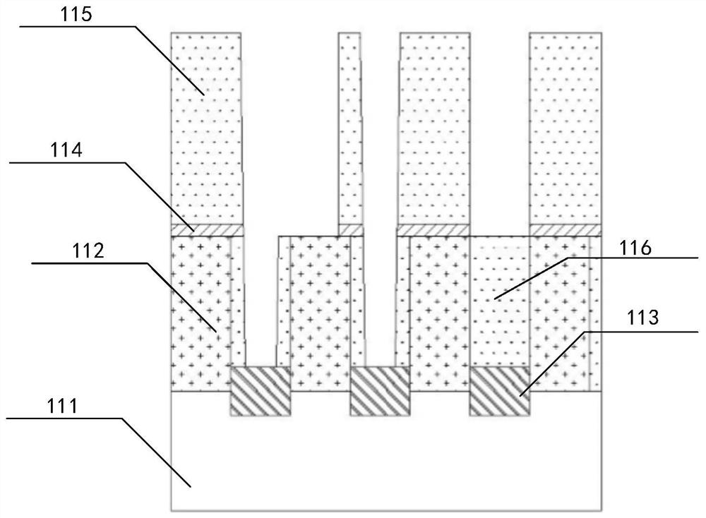
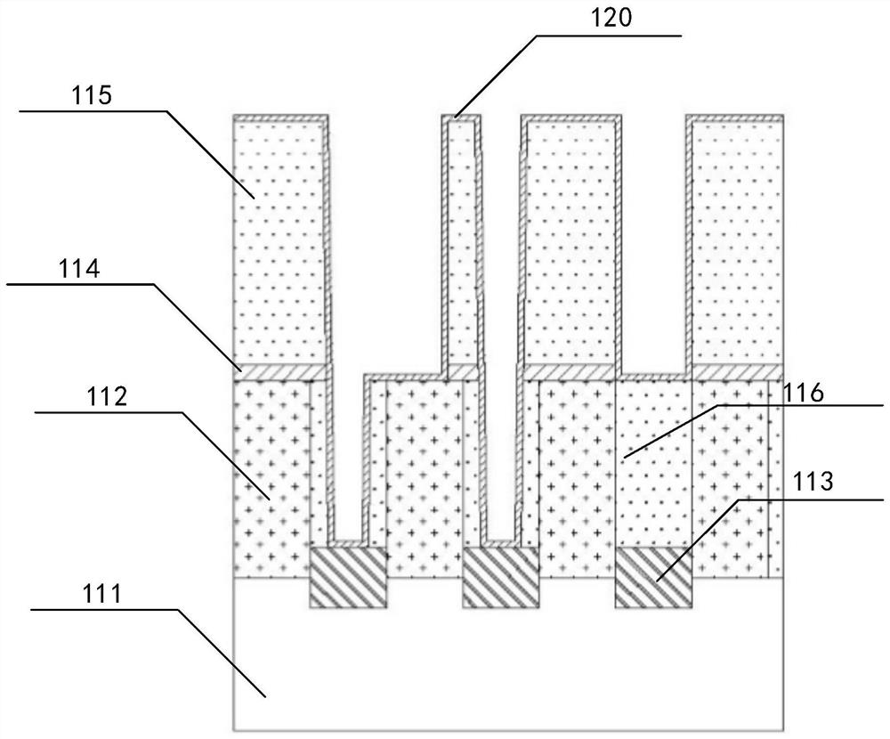
[0048] Please refer to Figure 1-Figure 5 , Figure 1 to Figure 5 It is a structural schematic diagram corresponding to each step in a method for forming a semiconductor structure.

[0049] Such as figure 1 As shown, a substrate is provided, and the substrate includes a substrate 111, a gate structure 112 on the substrate 111, source and drain doped regions 113 on both sides of the gate structure 112, and a 112 and the isolation layer 114 on the source-drain doped region 113, the first dielectric layer 115 and the second dielectric layer 116 above the isolation layer 114, and the second dielectric layer 116 is located adjacent to the gate between the electrode structures 112 ...


PUM


Abstract

According to the forming method of the semiconductor structure provided by the embodiment of the invention, the formation of the first trench exposing the source-drain doped region and the formation of the second trench located above the gate structure are realized through two steps, and when the second trench is formed, the isolation layer is used as a stop layer, so that the gate structure is not exposed, and the gate structure is not exposed. The first protection layer and the second protection layer are formed on the top surface of the gate structure instead of being protected by the isolation layer until the isolation layer and the first protection layer above the top surface of the gate structure are etched before the conductive plug is formed, and the gate structure is exposed. Therefore, according to the forming method of the semiconductor structure provided by the embodiment of the invention, the isolation layer and the first protection layer above the gate structure are removed only before the conductive plug is formed, so that the gate structure can be well protected, the exposure time of the gate structure is shortened, and the possibility of forming particle defects is reduced; therefore, the failure probability of the semiconductor structure is reduced, and the performance of the obtained semiconductor structure can be improved.

Description

technical field [0001] Embodiments of the present invention relate to the field of semiconductor manufacturing, and in particular, to a semiconductor structure and a method for forming the same. Background technique [0002] In the post-production process of the semiconductor device, it is usually necessary to form a metal interconnection structure, wherein the metal interconnection structure is used to connect the metal gate and the source-drain doped region. Therefore, before forming the metal interconnection structure, the metal gate to be connected needs to be exposed. [0003] However, if the metal gate is exposed for too long, grain defects may form, which in turn easily lead to structural failure and even damage to the resulting semiconductor structure. [0004] In the prior art, the metal gate cannot be well protected, which eventually leads to poor performance of the device formed by the existing semiconductor process. Contents of the invention [0005] The tech...

Claims


Application Information

Patent Timeline
Patent Type & Authority Applications(China)
IPC IPC(8): H01L21/768H01L23/48H01L21/8234H01L27/088
CPCH01L21/76805H01L21/76895H01L23/481H01L21/823475H01L27/088
Inventor 赵炳贵
Owner SEMICON MFG INT (SHANGHAI) CORP
Why Eureka
Try Eureka