Supercharge Your Innovation With Domain-Expert AI Agents!

Package structure and manufacturing method thereof

A packaging structure, flip-chip technology, applied in semiconductor/solid-state device manufacturing, semiconductor/solid-state device components, semiconductor devices, etc., can solve problems such as large chip size, lighter weight, chip warpage, etc., to increase strength and weight, avoid warping, achieve the effect of electromagnetic shielding

Pending Publication Date: 2022-05-10
SAMSUNG SEMICON CHINA RES & DEV +1
View PDF0 Cites 0 Cited by
  • Summary
  • Abstract
  • Description
  • Claims
  • Application Information

AI Technical Summary

Problems solved by technology

However, chips that consume a lot of power usually also have a large die size
After the chip is thinned, the weight will become lighter, which will lead to more serious chip warping problems, and even lead to virtual soldering problems

Method used


Image

  • Package structure and manufacturing method thereof
  • Package structure and manufacturing method thereof
  • Package structure and manufacturing method thereof

Examples


Embodiment Construction

[0023] Hereinafter, the present invention will be more fully described with reference to the accompanying drawings. As those skilled in the art would realize, the embodiments may be modified in various different ways, all without departing from the spirit or scope of the present invention. Irrelevant parts will be omitted to clearly describe the present invention.

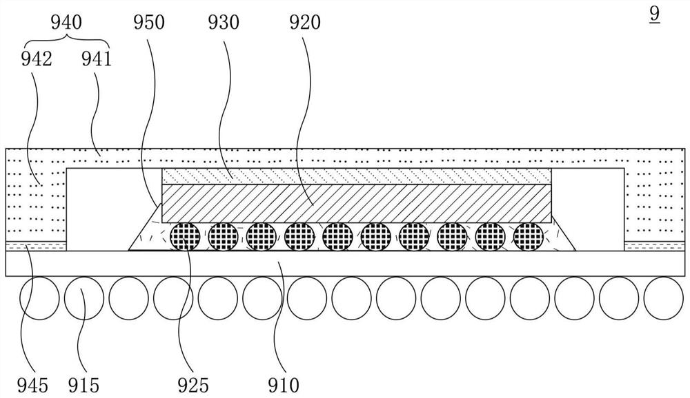
[0024] figure 2 is a cross-sectional view showing the package structure 1 according to the embodiment of the present invention.

[0025] The package structure 1 may include a substrate 110 and a chip 120 disposed on the substrate 110 in a flip-chip manner. Substrate 110 may include ceramic, glass, plastic, and / or other substrate materials. For example, the substrate 110 may include bismaleimide triazine (BT) resin. The side of the chip 120 that is electrically connected to the outside is the front side. exist figure 2 , the front side of the chip 120 corresponds to the lower surface of the chip 120 . The c...


PUM


Abstract

The invention provides a packaging structure and a manufacturing method thereof. The packaging structure comprises a substrate; the chip is mounted on the substrate in a flip chip manner; and a side heat sink including a thermally conductive material and disposed on a side surface of the chip. The side heat sink is electrically connected to the circuit layer of the chip.

Description

technical field [0001] Generally speaking, the present invention belongs to the field of semiconductor packaging; in particular, the present invention relates to a side heat dissipation enhanced packaging structure and a manufacturing method thereof. Background technique [0002] The heat generated by the power consumption of the chip will heat up the chip, which will affect the performance of the chip and even cause irreversible damage to the chip. Research on power consumption has always been carried out in all aspects of chip production, and the energy consumption ratio of chips has been improving with the improvement of design and progress of manufacturing process. However, the demand for chip performance is still increasing, so the improvement of energy consumption ratio cannot solve the heat dissipation problem caused by chip power consumption. Thermal issues are more pronounced in high-end chips (such as CPUs, GPUs, etc.). With the development of the manufacturing p...

Claims


Application Information

Patent Timeline
Patent Type & Authority Applications(China)
IPC IPC(8): H01L23/367H01L23/31H01L23/552H01L21/50H01L21/56
CPCH01L23/367H01L23/3675H01L23/3107H01L23/552H01L21/50H01L21/561H01L21/568H01L23/36H01L24/13H01L23/3736H01L23/562H01L21/6835H01L2221/68345H01L2221/68359H01L23/3128H01L24/16H01L24/11H01L24/17H01L24/09H01L23/3157H01L21/563H01L21/4882H01L21/52H01L23/433H01L2224/0401H01L23/3677H01L24/32H01L24/73H01L2224/119H01L2224/16225H01L2224/32225H01L2224/73204H01L2924/1616H01L2924/16195H01L2924/16235H01L2924/16251H01L2924/16315H01L2924/1632H01L2924/3511H01L2924/384
Inventor 朴龙浩黎英
Owner SAMSUNG SEMICON CHINA RES & DEV
Features
  • R&D
  • Intellectual Property
  • Life Sciences
  • Materials
  • Tech Scout
  • Unparalleled Data Quality
  • Higher Quality Content
  • 60% Fewer Hallucinations
Learn More