High-frequency surface acoustic wave resonator and preparation method thereof
A high-frequency surface acoustic wave and resonator technology, applied in the direction of impedance network, electrical components, etc., can solve the problems of high preferred orientation, thermal stress material deformation and cracking of multi-layer film structure, and achieve high electromechanical coupling coefficient, low working temperature, The effect of reducing thermal stress
Pending Publication Date: 2022-05-17
SOUTH CHINA UNIV OF TECH
View PDF3 Cites 0 Cited by
- Summary
- Abstract
- Description
- Claims
- Application Information
AI Technical Summary
Problems solved by technology
However, most of the piezoelectric films obtained by the deposition process are polycrystalline, and it is difficult to obtain a high preferred orientation, which leads to the generation of parasitic clutter and makes it difficult to control the frequency response of the device.
The single crystal piezoelectric thin film is generally prepared by direct bonding process, but this process generally requires annealing at a temperature greater than 400°C. Due to the different thermal expan
Method used
View moreImage
Smart ImageViewing Examples

Examples
 PUM
 Abstract
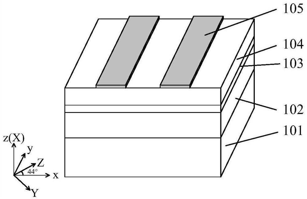
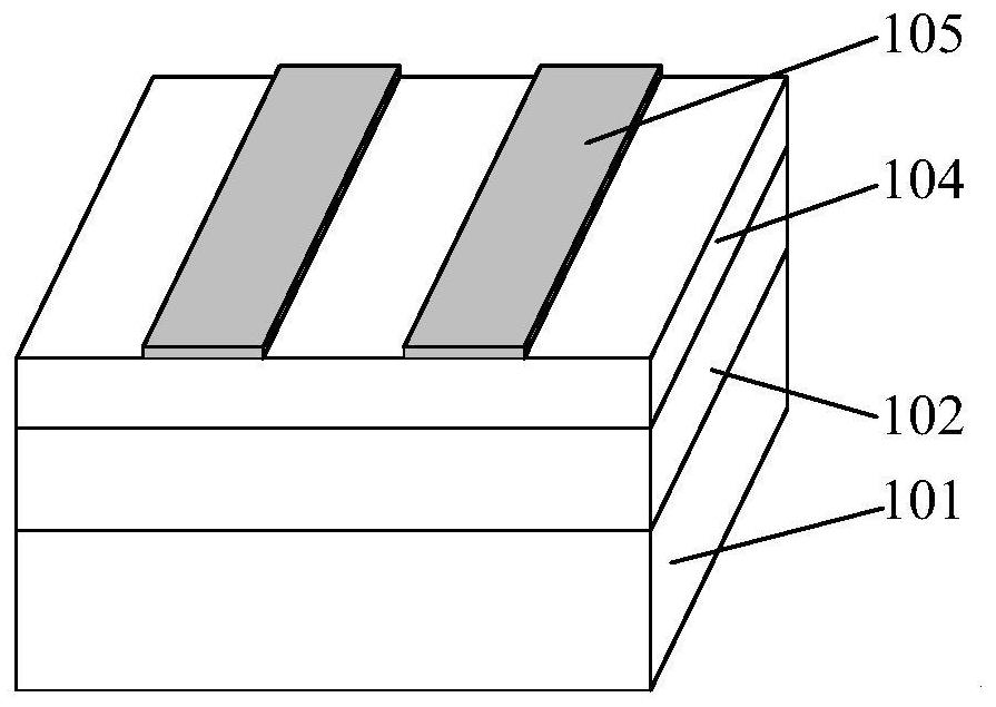
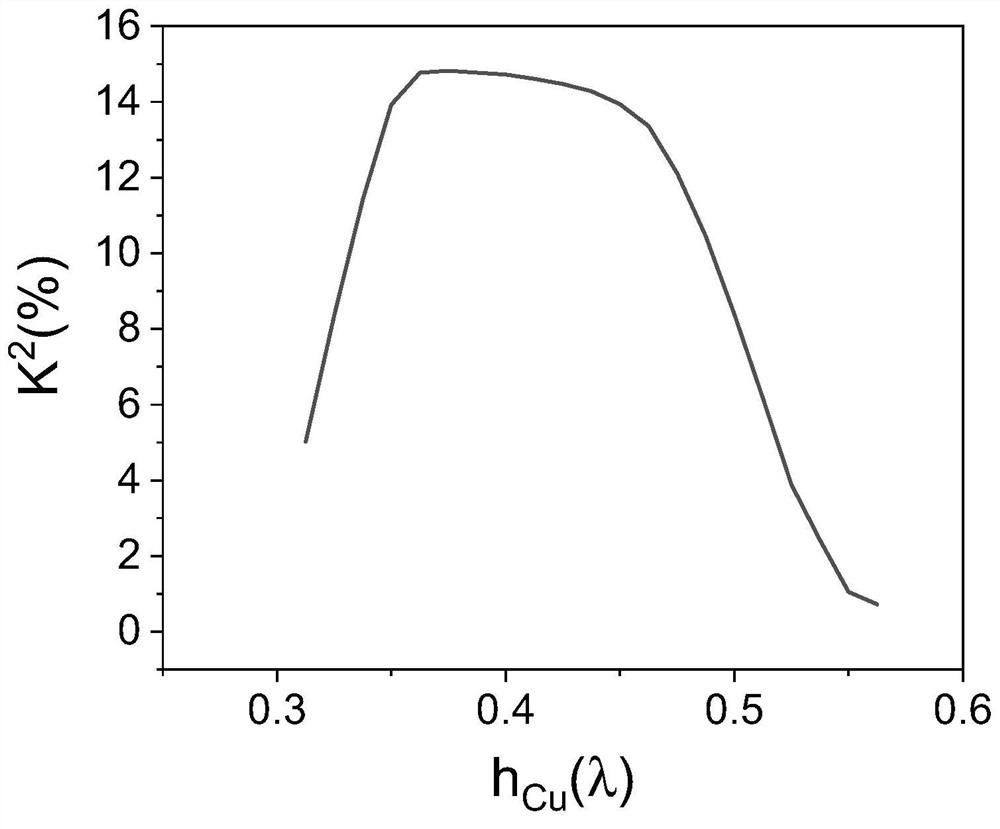
The invention discloses a high-frequency surface acoustic wave resonator and a preparation method thereof, relates to a microelectronic device for 5G communication, and provides the scheme for solving the problems of high bonding transfer temperature, low electromechanical coupling coefficient and the like in the prior art. A first bonding metal layer is arranged on the end face, away from the first substrate, of the high-sound-velocity substrate, a second bonding metal layer is arranged on the end face, away from the interdigital electrode, of the piezoelectric film, and bonding processing of the piezoelectric film and the high-sound-velocity substrate is completed through the first bonding metal layer and the second bonding metal layer. The method has the advantages that the method is compatible with a low-temperature metal bonding process, the working temperature of metal bonding is lower, and the thermal stress of a device can be greatly reduced. And secondly, metal bonding can enable a bonding interface to obtain higher bonding energy, and the device is more stable. Besides, the X-cut lithium niobate is used as the piezoelectric film, and the included angle of 44 degrees is formed between the vertical direction of the interdigital electrode and the Z axis of the piezoelectric film, so that a higher electromechanical coupling coefficient can be obtained, and the bandwidth of the device is improved.
Description
technical field [0001] The invention relates to a microelectronic device for 5G communication, in particular to a high-frequency surface acoustic wave resonator and a preparation method thereof. Background technique [0002] Surface acoustic wave resonators (SAW) are widely used in the field of wireless communications. However, with the development of wireless communication technologies such as social networks and the Internet of Things and the rapid growth of related business requirements, especially the arrival of 5G mobile communications, it is required that acoustic wave resonators work in Higher frequency and greater bandwidth. However, when the frequency of the surface acoustic wave resonator increases, its bandwidth decreases rapidly and the loss increases. Therefore, the operating frequency of the current surface acoustic wave resonator is generally lower than 3GHz. In order to meet the needs of 5G communication, how to improve the operating frequency and bandwidth ...
Claims
Login to View More Application Information
Patent Timeline
 IPC IPC(8): H03H9/25H03H3/08H03H9/02H03H9/145
CPCH03H9/25H03H3/08H03H9/02559H03H9/145Y02D30/70
Inventor 周长见李丹花郭思聪张传俊邓永健
Owner SOUTH CHINA UNIV OF TECH
Features
- R&D
- Intellectual Property
- Life Sciences
- Materials
- Tech Scout
- Unparalleled Data Quality
- Higher Quality Content
- 60% Fewer Hallucinations
Learn More Browse by: Latest US Patents, China's latest patents, Technical Efficacy Thesaurus, Application Domain, Technology Topic, Popular Technical Reports.
© 2025 PatSnap. All rights reserved.Legal|Privacy policy|Modern Slavery Act Transparency Statement|Sitemap|About US| Contact US: help@patsnap.com