

LED chip and manufacturing method thereof
An LED chip and epitaxy technology, applied in semiconductor devices, electrical components, circuits, etc., can solve problems such as current congestion, and achieve the effects of facilitating production, enhancing reliability, and inhibiting electrochemical hydrolysis
- Summary
- Abstract
- Description
- Claims
- Application Information
AI Technical Summary
Problems solved by technology
Method used
Image

Examples
Embodiment Construction
[0043] In order to make the content of the present invention clearer, the content of the present invention will be further described below with reference to the accompanying drawings. The present invention is not limited to this specific embodiment. Based on the embodiments of the present invention, all other embodiments obtained by those of ordinary skill in the art without creative efforts shall fall within the protection scope of the present invention.
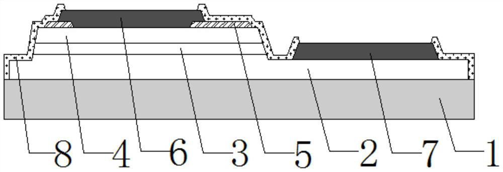
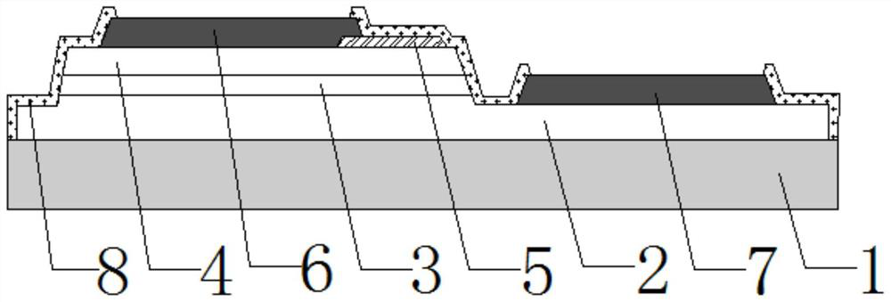
[0044] like image 3 As shown, an LED chip includes:
[0045] substrate 1;
[0046] An epitaxial stack L disposed on the surface of the substrate 1, the epitaxial stack L includes a first-type semiconductor layer 2, an active region 3 and a second-type semiconductor layer 4 stacked in sequence along a first direction, and a part of the epitaxial stack L The region is etched to a part of the first type semiconductor layer 2 to form a groove L1 and a light-emitting mesa L2, wherein the light-emitting mesa L2 has edges and ...
PUM
 Abstract
Description
Claims
Application Information