A high aspect ratio circuit board through-hole electroplating process

A through-hole electroplating, high aspect ratio technology, applied in electrodes, printed circuits, electrical components, etc., can solve the problem of uneven current density distribution in the hole/hole center, uneven copper deposition in the hole/hole center, and long-term products. Reliability risks and other issues, to achieve the effect of improving deep plating capacity, reducing anode oxygen evolution, and maintaining stability

Active Publication Date: 2022-07-19
SHENZHEN BANMING SCI & TECH CO LTD
View PDF0 Cites 0 Cited by
  • Summary
  • Abstract
  • Description
  • Claims
  • Application Information

AI Technical Summary

Problems solved by technology

In traditional DC electroplating, the uneven distribution of current density at the orifice / hole center caused by the ohmic effect and the edge effect often causes the phenomenon that the coating thickness of the tiny through-hole gradually decreases from the orifice to the center of the hole, resulting in the orifice / hole center. The copper deposition in the center of the hole is extremely uneven, forming a dog-bone-shaped coating, and even sealing the hole in severe cases, making it difficult to achieve good interconnection between layers
Traditional DC electroplating is generally only suitable for through-hole copper plating with a thickness-to-diameter ratio below 8:1, and cannot meet this type of product.
For this type of through-hole with high thickness-to-diameter ratio, many companies use the method of first copper plating and then surface copper reduction, which not only leads to a long manufacturing process and high cost, but also brings risks to the long-term reliability of the product.

Method used


Image

  • A high aspect ratio circuit board through-hole electroplating process
  • A high aspect ratio circuit board through-hole electroplating process
  • A high aspect ratio circuit board through-hole electroplating process

Examples


Embodiment 1

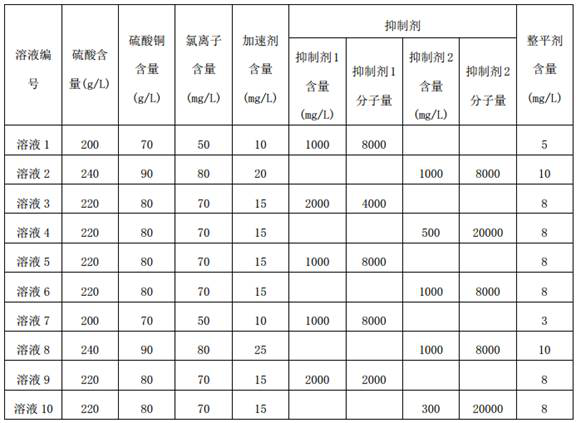
[0030] A copper electroplating solution for high aspect ratio circuit board through-hole electroplating, the copper electroplating solution is composed of the following components: sulfuric acid 200-240g / L, copper sulfate pentahydrate 70-90g / L, chloride ion 50- 80ppm, accelerator 10-20ppm, inhibitor 500-2000ppm, leveling agent 5-10ppm. Described accelerator is isothiourea propanesulfonic acid inner salt, specifically, can select molecular formula to be C 4 H 10 N 2 O 3 S 2 The isothiourea propanesulfonic acid inner salt; the inhibitor is polyethylene glycol or polyethylene glycol ether, the molecular weight of the inhibitor is 4000-20000; the leveling agent is a specific thiadiazole amide compound , the structural formula of the specific thiadiazole amide compound is:

[0031] .

Embodiment 2

[0033] The through-hole electroplating was performed using the electroplating copper solution suitable for the high aspect ratio circuit board through-hole electroplating process of Example 1, specifically, electroplating using forward and reverse pulse currents. A titanium anode coated with iridium and tantalum is used as the anode, and the electroplating process conditions are: the forward current density is 1.2-1.8 A / dm 2 , the forward and reverse pulse current amplitude ratio is 1:2-1:3; the forward pulse time is 100-200 milliseconds, and the forward and reverse pulse time ratio is 10:1-20:1; during electroplating, the solution temperature is 10 -35°C.


PUM


Abstract

The invention relates to a high aspect ratio circuit board through hole electroplating process, and relates to the technical field of circuit board electroplating. A high aspect ratio circuit board through-hole electroplating process, comprising the following steps: using a titanium anode whose surface is coated with iridium and tantalum as an anode, and performing pulse electroplating on the circuit board provided with the through-hole in a copper electroplating solution; The pulse electroplating is forward and reverse pulse current electroplating, and the process conditions are: the forward current density is 1.2-1.8 A / dm 2 , the forward and reverse pulse current amplitude ratio is 1:2‑1:3; the forward pulse time is 100‑200 milliseconds, and the forward and reverse pulse time ratio is 10:1‑20:1; the copper electroplating solution is composed of the following Concentration of components: sulfuric acid 200-240g / L, copper sulfate pentahydrate 70-90g / L, chloride ion 50-80ppm, accelerator 10-20ppm, inhibitor 500-2000ppm and leveling agent 5-10ppm. The high aspect ratio circuit board through-hole electroplating process of the present application can effectively improve the uniformity of the plating layer on the surface of the circuit board and in the hole, reduce the thickness difference between the copper thickness in the circuit board hole and the copper thickness on the circuit board surface, and improve the deep plating ability. .

Description

technical field [0001] The invention relates to the technical field of circuit board electroplating, in particular to a high aspect ratio circuit board through-hole electroplating process. Background technique [0002] With the accelerated construction of network infrastructure such as 5G base stations, the demand for communication printed circuit boards has increased. In the 5G base station, the communication backplane is the core circuit board in the mobile base station. The development trend of the communication backplane is that the number of bearing sub-boards is increasing and the signal loss is decreasing. More, thicker plate thickness, smaller aperture, and denser wiring. The thickness / number of layers of the multi-layer communication backplane is increasing, while the aperture is decreasing, resulting in an increasing aspect ratio of the board and an increasing number of products with an aspect ratio (>14:1). The difficulty of copper plating of tiny through-hol...

Claims


Application Information

Patent Timeline
Patent Type & Authority Patents(China)
IPC IPC(8): C25D3/38C25D5/18C25D7/00C25D17/10H05K3/42
CPCC25D3/38C25D5/18C25D7/00C25D17/10H05K3/424
Inventor 宗高亮谢慈育李得志
Owner SHENZHEN BANMING SCI & TECH CO LTD
Why Eureka
Try Eureka