Forming method of bulk acoustic wave resonance device

A resonant device, bulk acoustic wave technology, applied in the direction of impedance network, electrical components, etc., to achieve the effect of avoiding process technology, reducing production cost, and improving Q value

Pending Publication Date: 2022-06-07
CHANGZHOU CHEMSEMI CO LTD
View PDF0 Cites 0 Cited by
  • Summary
  • Abstract
  • Description
  • Claims
  • Application Information

AI Technical Summary

Problems solved by technology

[0005] However, there are still many problems in the bul

Method used


Image

  • Forming method of bulk acoustic wave resonance device
  • Forming method of bulk acoustic wave resonance device
  • Forming method of bulk acoustic wave resonance device

Examples


Embodiment Construction

[0038] As mentioned in the background art, the bulk acoustic wave resonance device formed in the prior art still has many problems. The following will be described in detail with reference to the accompanying drawings.

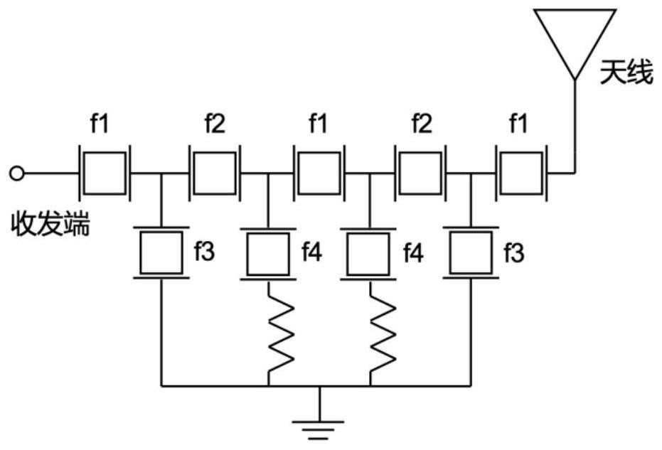
[0039] figure 1 is a schematic diagram of a bulk acoustic wave filter circuit; figure 2 It is a schematic diagram of the structure of a thin film bulk acoustic wave resonator.

[0040] Please refer to figure 1 , a bulk acoustic wave filter circuit, including a ladder circuit composed of a plurality of bulk acoustic wave resonators, wherein f1, f2, f3, f4 respectively represent four different frequencies. In each bulk acoustic wave resonator, the metal electrodes on both sides of the piezoelectric layer of the resonator generate alternating positive and negative voltages, and the piezoelectric layer generates acoustic waves through alternating positive and negative voltages, and the acoustic waves in the resonator propagate in a direction perpendicular to t...


PUM

PropertyMeasurementUnit
Thicknessaaaaaaaaaa
Thicknessaaaaaaaaaa

Abstract

A forming method of a bulk acoustic wave resonance device comprises the following steps: providing a substrate; forming an intermediate layer on the substrate; forming a first opening embedded in the intermediate layer; forming a sacrificial layer in the first opening, wherein the top surface of the sacrificial layer is flush with the top surface of the intermediate layer; forming a second opening, and embedding the intermediate layer and the sacrificial layer; forming a first electrode layer in the second opening, wherein the top surface of the first electrode layer is flush with the top surface of the intermediate layer; forming a piezoelectric layer on the intermediate layer, the sacrificial layer and the first electrode layer; and forming a second electrode layer on the piezoelectric layer. The top surfaces of the intermediate layer, the sacrificial layer and the first electrode layer are flush, so that the formed piezoelectric layer does not comprise obviously turned crystal grains, and the electromechanical coupling coefficient of the resonance device and the Q value of the resonance device can be improved. In addition, the bulk acoustic wave resonance device is formed in a layer stacking mode, the bonding process is avoided, the manufacturing steps are effectively simplified, and the manufacturing cost is reduced.

Description

technical field [0001] The present invention relates to the technical field of semiconductor manufacturing, and in particular, to a method for forming a bulk acoustic wave resonance device. Background technique [0002] A radio frequency (Radio Frequency, RF) front-end chip of a wireless communication device includes a power amplifier, an antenna switch, a radio frequency filter, a multiplexer including a duplexer, a low noise amplifier, and the like. Among them, the radio frequency filter includes surface acoustic wave (Surface Acoustic Wave, SAW) filter, bulk acoustic wave (Bulk Acoustic Wave, BAW) filter, Micro-Electro-Mechanical System (Micro-Electro-Mechanical System, MEMS) filter, integrated passive Device (Integrated Passive Devices, IPD) filter and so on. [0003] The quality factor value (Q value) of SAW resonators and BAW resonators is high, and the RF filters with low insertion loss and high out-of-band suppression made of SAW resonators and BAW resonators, namel...

Claims


Application Information

Patent Timeline
IPC IPC(8): H03H3/02
CPCH03H3/02H03H2003/023
Inventor 邹雅丽周建韩兴王斌
Owner CHANGZHOU CHEMSEMI CO LTD
Why Eureka
Try Eureka