Color image sensor with two layers of stacked pixels and color arrangement array thereof
A color image, stacking technology, applied in semiconductor devices, electric solid state devices, radiation control devices, etc., can solve the problems of low light transmittance of silicon, complex production process and high cost
Pending Publication Date: 2022-06-21
深圳市康睿优医疗器械有限公司
View PDF0 Cites 0 Cited by
- Summary
- Abstract
- Description
- Claims
- Application Information
AI Technical Summary
Problems solved by technology
[0006] The image effect of the above-mentioned color image sensor using three-layer stacked pixels is indeed better than the above-mentioned most common color image sensor using single-layer pixels, but due to the low light transmittance of silicon, the bottom pixel (generally imaging red light) ) The image quality is poor; and because its production process is too complex, the number of circuits and analog-to-digital converters (ADC) is large, resulting in high cost, which is not conducive to popularization
Method used
View moreImage
Smart ImageViewing Examples

Examples
Embodiment Construction
Login to view more PUM
 Abstract
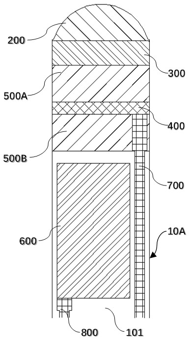
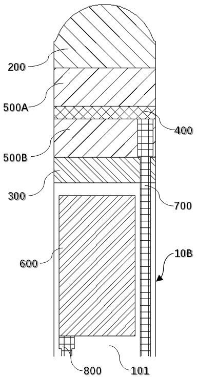
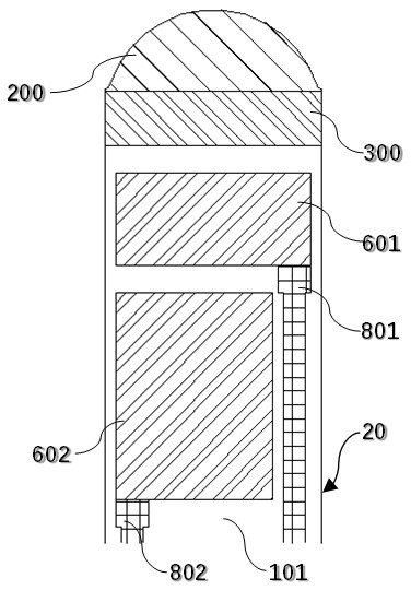
According to the color image sensor, all or part of pixels of the color image sensor adopt two-layer stacked pixels, and the two-layer stacked pixels at least comprise a semiconductor substrate; the photoelectric conversion unit 1 is arranged in the semiconductor substrate, and part of light which is not subjected to photoelectric conversion and passes through the optical filter and the photoelectric conversion unit 2 on the semiconductor substrate reaches the photoelectric conversion unit 1 in the semiconductor substrate; the photoelectric conversion unit 2 is arranged on the semiconductor substrate and at least comprises a photoelectric conversion layer and two electrodes, and the photoelectric conversion layer is used for performing photoelectric conversion on light in a specific wavelength range; the optical filter may be positioned between the photoelectric conversion unit (1) and the photoelectric conversion unit (2) to control the wavelength range of light reaching the photoelectric conversion unit (1), or may be positioned on the photoelectric conversion unit (2) to control the wavelength range of the total light reaching the photoelectric conversion unit (1) and the photoelectric conversion unit (2).
Description
technical field [0001] The present invention relates to a color image sensor with two layers of stacked pixels, and its color arrangement array. Background technique [0002] As a device that converts optical signals into electrical signals and realizes digitization, CCD and CMOS image sensors, especially CMOS color image sensors, have been widely used in digital cameras, smart phones, tablet computers, unmanned driving, artificial intelligence and other fields. [0003] The most common color image sensor uses a photosensitive diode with a color filter (Color Filter) on it to limit the wavelength range of the incident light, that is, the color of the incident light, so that each pixel can only sample red, green and blue colors. A color filter array (Color Filter Array) is set for the entire image sensor to realize the acquisition of color images. Among these color filter arrays, the Bayer (Bayer) filter array is the most common, and this array loses 1 / 2 of green light, 3 / 4 ...
Claims
Login to view more Application Information
Patent Timeline
 IPC IPC(8): H01L27/146
CPCH01L27/14605H01L27/1461H01L27/14621H01L27/14627H01L27/14641
Inventor 潘欢
Owner 深圳市康睿优医疗器械有限公司
- R&D Engineer
- R&D Manager
- IP Professional
Why Eureka
- Industry Leading Data Capabilities
- Powerful AI technology
- Patent DNA Extraction
Try Eureka
Browse by: Latest US Patents, China's latest patents, Technical Efficacy Thesaurus, Application Domain, Technology Topic.
© 2024 PatSnap. All rights reserved.Legal|Privacy policy|Modern Slavery Act Transparency Statement|Sitemap