Stress buffering packaging structure of MEMS device
A stress buffering and packaging structure technology, applied in microstructure technology, electric solid devices, semiconductor devices, etc., can solve the problems of low structural strength, low rigidity, not suitable for high overload applications, etc., to achieve high packaging stress and consistent improvement properties, reducing the effect of stress coupling
- Summary
- Abstract
- Description
- Claims
- Application Information
AI Technical Summary
Problems solved by technology
Method used
Image
Examples
Embodiment 1
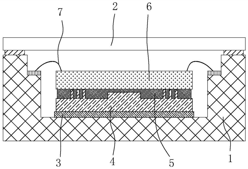
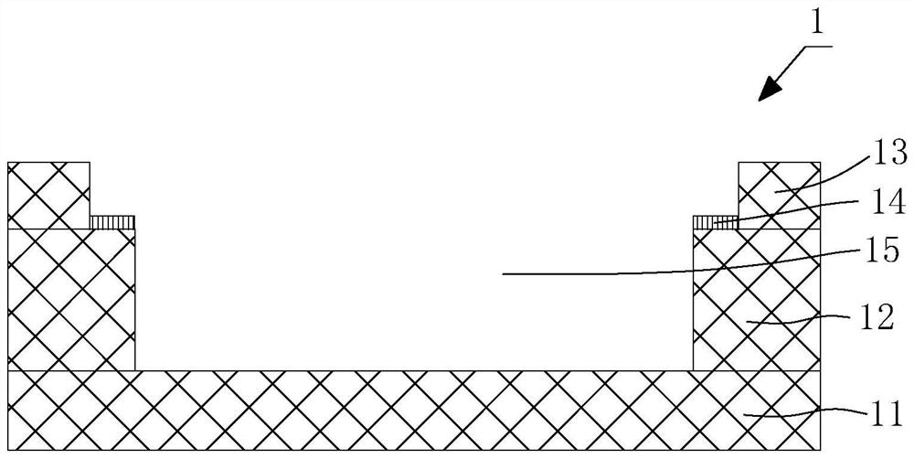
[0033] A stress buffer package structure of a MEMS device, refer to Figure 1 to Figure 4 , which includes a package tube 1 and a MEMS chip 6, the package tube 1 is fixedly provided with a stress buffer pad 4 for carrying the MEMS chip 6, and an adhesive sheet is arranged between the stress buffer pad 4 and the MEMS chip 6; stress; The buffer plate 4 includes a substrate 41, and the end face of the substrate 41 opposite to the MEMS chip 6 is provided with at least two protrusions with different heights; the substrate 41 is matched with at least two protrusions with different heights, so that A three-dimensional pattern feature is formed on the front side of the stress buffer pad 4, which is used to fix the adhesive to a specific shape, which can not only realize the bonding and fixing of the MEMS chip, but also greatly reduce the stress between the MEMS chip and the package shell. It can provide sufficient bonding strength to the MEMS chip, and greatly improve the consistency ...
Embodiment 2
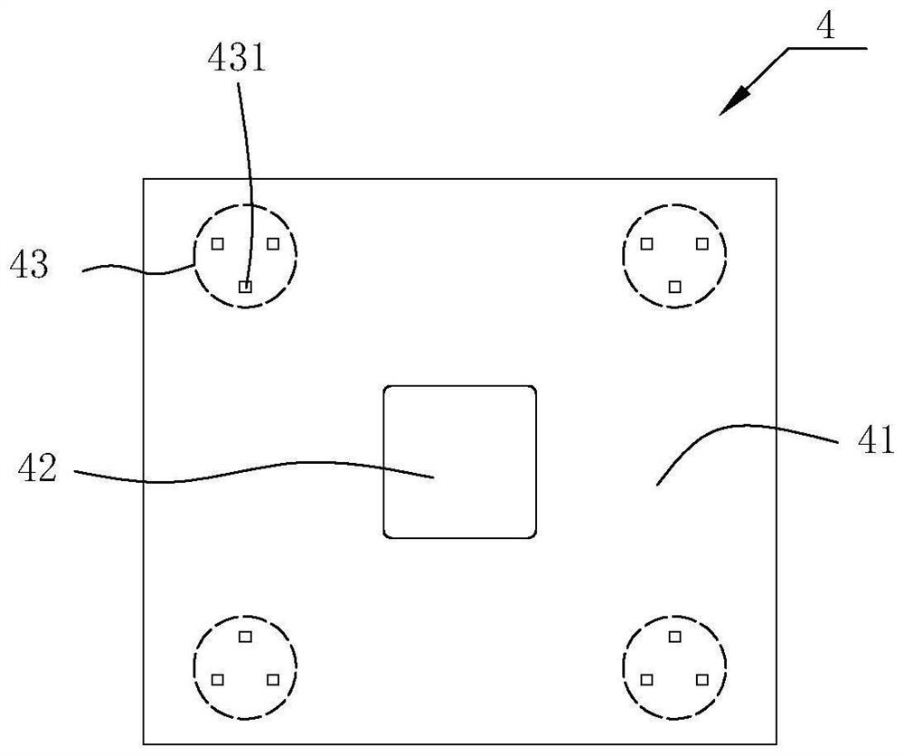
[0043] A stress buffer package structure of a MEMS device, refer to Figure 5 , on the basis of Embodiment 1, the difference between this embodiment and Embodiment 1 is that in this embodiment, a boss 42 and three bump circles 43 are provided on the substrate 41, and the boss 42 and the three bumps The circles 43 are respectively arranged at the four top corners of the substrate 41 , and the heights of the substrate 41 , the bosses 42 and the bumps 431 increase to form another three-dimensional graphic feature on the front surface of the stress buffer plate 4 .
Embodiment 3
[0045] A stress buffer package structure of a MEMS device, refer to Figure 1 to Figure 4 as well as Image 6 , Based on Embodiment 1, the difference between this embodiment and Embodiment 1 is that in this embodiment, the second adhesive for bonding the MEMS chip 6 does not use the whole surface bonding, and is bonded at multiple points. is five glue points, including the boss glue point 51 and the bump circle glue point 52; the position and shape of the five glue points are determined by the position and shape of the boss 42 and the bump circle 43, namely The area of the boss glue point 51 is about the area of the boss 42, the glue thickness is equal to the first height difference, the diameter of the bump ring glue point 52 is about the diameter of the bump circle 43, and the glue thickness is the first height difference and the The sum of the second height difference; compared with Example 1, the stress buffering or releasing effect can be improved.
[0046] refer to...
PUM
| Property | Measurement | Unit |
|---|---|---|
| diameter | aaaaa | aaaaa |
| diameter | aaaaa | aaaaa |
| thickness | aaaaa | aaaaa |
Abstract
Description
Claims
Application Information
 - R&D
- Intellectual Property
- Life Sciences
- Materials
- Tech Scout
- Unparalleled Data Quality
- Higher Quality Content
- 60% Fewer Hallucinations
Browse by: Latest US Patents, China's latest patents, Technical Efficacy Thesaurus, Application Domain, Technology Topic, Popular Technical Reports.
© 2025 PatSnap. All rights reserved.Legal|Privacy policy|Modern Slavery Act Transparency Statement|Sitemap|About US| Contact US: help@patsnap.com


