Supercharge Your Innovation With Domain-Expert AI Agents!

Reference buffer circuit, ADC system, receiver, base station and mobile device

A buffer circuit and buffer amplifier technology, applied in logic circuits, transmission systems, pulse technology, etc., can solve problems such as output kickback

Pending Publication Date: 2022-06-24
INTEL CORP
View PDF0 Cites 0 Cited by
  • Summary
  • Abstract
  • Description
  • Claims
  • Application Information

AI Technical Summary

Problems solved by technology

But the source follower suffers from gate-source capacitance coupling the output of the buffer to the bias potential and causing the output to kick back to the bias line

Method used


Image

  • Reference buffer circuit, ADC system, receiver, base station and mobile device
  • Reference buffer circuit, ADC system, receiver, base station and mobile device
  • Reference buffer circuit, ADC system, receiver, base station and mobile device

Examples


example 1

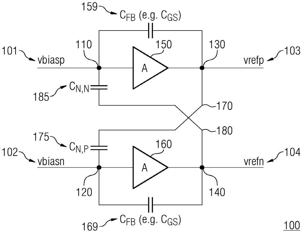
[0103] Example 1 is a reference buffer circuit for an analog-to-digital converter, the reference buffer circuit comprising: a first input node configured to receive a first bias signal of a first polarity from a first signal line; a second input a node configured to receive a second bias signal of a second polarity from a second signal line; a first output node configured to output a first reference signal of a first polarity, wherein the first buffer amplifier is coupled to the first between an input node and a first output node; a second output node configured to output a second reference signal of a second polarity, wherein a second buffer amplifier is coupled between the second input node and the second output node; the first a coupling path including a first capacitive element, wherein the first coupling path is coupled between the first output node and the second input node; and a second coupling path including a second capacitive element, wherein the second coupling path...

example 2

[0104] Example 2 is the reference buffer circuit of example 1, wherein the capacitance of the first capacitive element is equal to the capacitance of the second capacitive element.

example 3

[0105] Example 3 is the reference buffer circuit of example 1 or example 2, wherein the minimum corresponding capacitance of at least one of the first capacitive element and the second capacitive element is the gate-source of any transistor of the first buffer amplifier 50% of the capacitance, the maximum is 150% of it.


PUM


Abstract

A reference buffer circuit, an ADC system, a receiver, a base station, and a mobile device are provided. The reference buffer circuit includes a first input node that receives a first bias signal of a first polarity from a first signal line. The reference buffer circuit includes a second input node that receives a second bias signal of a second polarity from a second signal line. In addition, the reference buffer circuit includes a first output node that outputs a first reference signal. The first buffer amplifier is coupled between the first input node and the first output node. The reference buffer circuit further includes a second output node that outputs a second reference signal. A second buffer amplifier is coupled between the second input node and the second output node. The reference buffer circuit includes a first coupling path including a first capacitive element. The first coupling path is coupled between the first output node and the second input node. The reference buffer circuit includes a second coupling path including a second capacitive element. The second coupling path is coupled between the second output node and the first input node.

Description

technical field [0001] Examples of the invention relate to reference buffers for analog-to-digital converters (ADCs). Specifically, examples relate to reference buffer circuits for ADCs, ADC systems including reference buffer circuits, receivers including ADC systems, base stations including receivers, and mobile devices including receivers. Background technique [0002] In ADCs such as time-interleaved or pipelined ADCs, significant crosstalk can occur between sub-ADC references. In some implementations, each sub-ADC has its own reference buffer to allow some isolation of the reference voltages between the sub-ADCs. One of the simplest buffer circuits is the source follower. Due to the low output impedance, the source follower is simple, small, power efficient and broadband. But the source follower suffers from the gate-source capacitance coupling the output of the buffer to the bias potential and causing the output to kick back to the bias line. [0003] Therefore, the...

Claims


Application Information

Patent Timeline
Patent Type & Authority Applications(China)
IPC IPC(8): H03M1/08H04B1/40H04W88/08H03M1/12
CPCH03M1/0863H04B1/40H04W88/08H03M1/1245H03M1/0845H03M1/1215H03F3/30H03K19/00384H03K19/018578H03M1/0827H04B1/12
Inventor D·格吕贝尔C·林霍尔姆M·克拉拉G·卡肖
Owner INTEL CORP
Features
  • R&D
  • Intellectual Property
  • Life Sciences
  • Materials
  • Tech Scout
  • Unparalleled Data Quality
  • Higher Quality Content
  • 60% Fewer Hallucinations
Learn More