
Eureka
For R&D, Eureka makes reading and utilizing patents & technical documents easy.
Eureka AIR
Designed for self-driven R&D workflows. Generate viable solutions, solve complex R&D challenges, empower your innovation with AI.

Eureka Materials
Designed for material experts only. Revolutionize your material R&D, from search, analyze, to developing new materials.

TechResearch
Generate reliable direction feasibility study reports for your R&D in just a few steps.

TechSeek
Discover and master advanced knowledge NOW. Basics, ideas, possibilities, all at once.

TechMind
As an expert in R&D Theories, TechMind can generates customized viable solutions instantly.

TechRisk
Analyze your overall solution with one click, know your potential R&D risks in advance.

TechMonitor
Get weekly tech updates, stay abreast of the latest tech innovations and key insights.
Substrate structure and electronic device
A substrate structure and substrate technology, applied in the direction of circuits, electrical components, electrical solid devices, etc., can solve the problems of environmental pollution of electroplating solution, complex process, high cost, etc., and achieve the effect of simple production process, wide application and low cost
- Summary
- Abstract
- Description
- Claims
- Application Information
AI Technical Summary
Problems solved by technology
Method used
Image

Examples
Embodiment Construction
[0060] The substrate structure and the electronic device according to the preferred embodiments of the present invention will be described below with reference to the related drawings, wherein the same components will be described with the same reference numerals.
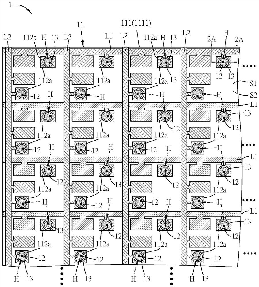
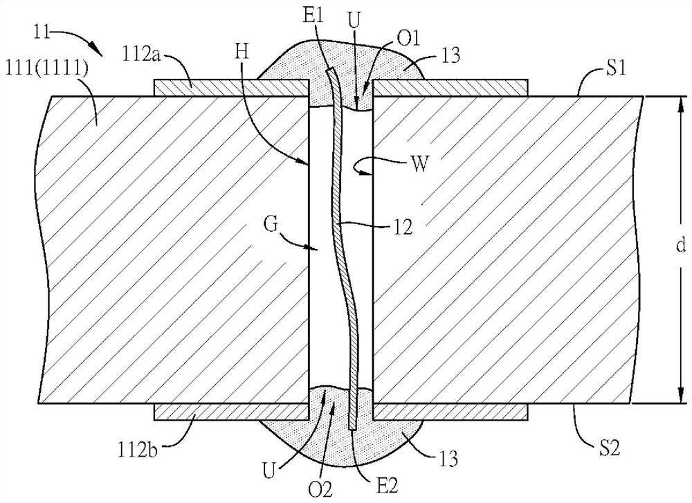
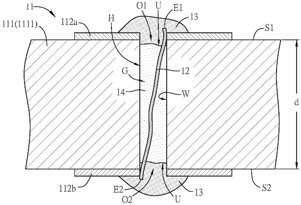
[0061] figure 1 is a schematic diagram of a substrate structure according to an embodiment of the present invention, and 2A to 2C respectively figure 1 Schematic cross-sectional views of different embodiments of the substrate structure along the secant line 2A-2A. like figure 1 As shown, the substrate structure in this embodiment is an active matrix (AM) substrate structure as an example, but it is not limited to this. In different embodiments, the substrate structure may also be passive Matrix (Passive Matrix, AM) substrate structure, or other types of substrate structure.
[0062] Please refer to figure 1 , 2A to 2C As shown, the substrate structure 1 includes a substrate 11 , a plurality of conductive li...
PUM
| Property | Measurement | Unit |
|---|---|---|
| thickness | aaaaa | aaaaa |
| pore size | aaaaa | aaaaa |
Abstract
Description
Claims
Application Information
 - R&D Engineer
- R&D Manager
- IP Professional
- Industry Leading Data Capabilities
- Powerful AI technology
- Patent DNA Extraction
Browse by: Latest US Patents, China's latest patents, Technical Efficacy Thesaurus, Application Domain, Technology Topic, Popular Technical Reports.
© 2024 PatSnap. All rights reserved.Legal|Privacy policy|Modern Slavery Act Transparency Statement|Sitemap|About US| Contact US: help@patsnap.com