High-luminous-efficiency LED chip and preparation method thereof

A LED chip, high light efficiency technology, applied in the direction of semiconductor devices, electrical components, circuits, etc., can solve the problems of production yield decline, small process window, high production yield, etc., to reduce light absorption, increase process window, light efficiency Enhanced effect

Pending Publication Date: 2022-07-05
JIANGXI ZHAO CHI SEMICON CO LTD
View PDF0 Cites 0 Cited by
  • Summary
  • Abstract
  • Description
  • Claims
  • Application Information

AI Technical Summary

Problems solved by technology

[0005] Aiming at the deficiencies of the prior art, the purpose of the present invention is to provide a high-efficiency LED chip and its preparation method, aiming to solve the problem that in the process of manufacturing LEDs in the prior art, due to the small process window, it is easy to lead to a decline in the production yield, which cannot be guaranteed. high production yield

Method used


Image

  • High-luminous-efficiency LED chip and preparation method thereof
  • High-luminous-efficiency LED chip and preparation method thereof

Examples


Embodiment 1

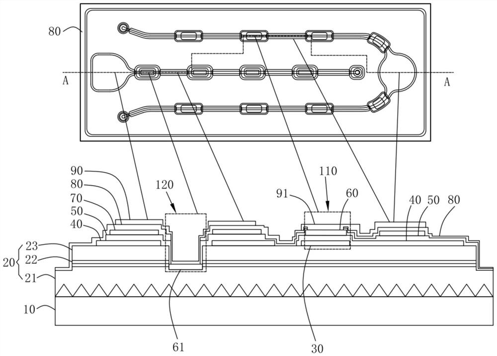
[0033] see figure 1 , the first embodiment of this aspect provides a high light efficiency LED chip, the chip includes a substrate 10 and an epitaxial layer 20, the epitaxial layer 20 includes an N-type semiconductor layer 21, a multiple quantum well region 22 and a P-type semiconductor layer layer 23;

[0034] The chip further includes a current blocking layer 30 provided on the P-type semiconductor layer 23 , a transparent conductive layer 40 provided on the current blocking layer 30 , and a first metal barrier provided on the transparent conductive layer 40 . layer 60 and the second metal barrier layer 61 provided on the N-type semiconductor layer 21 , the first insulating layer 50 provided on the transparent conductive layer 40 , the high reflection layer provided on the first insulating layer 50 a metal layer 70 and a second insulating layer 80 disposed on the high-reflection metal layer 70, the high-reflection metal layer 70 is kept insulated from the metal barrier laye...

Embodiment 2

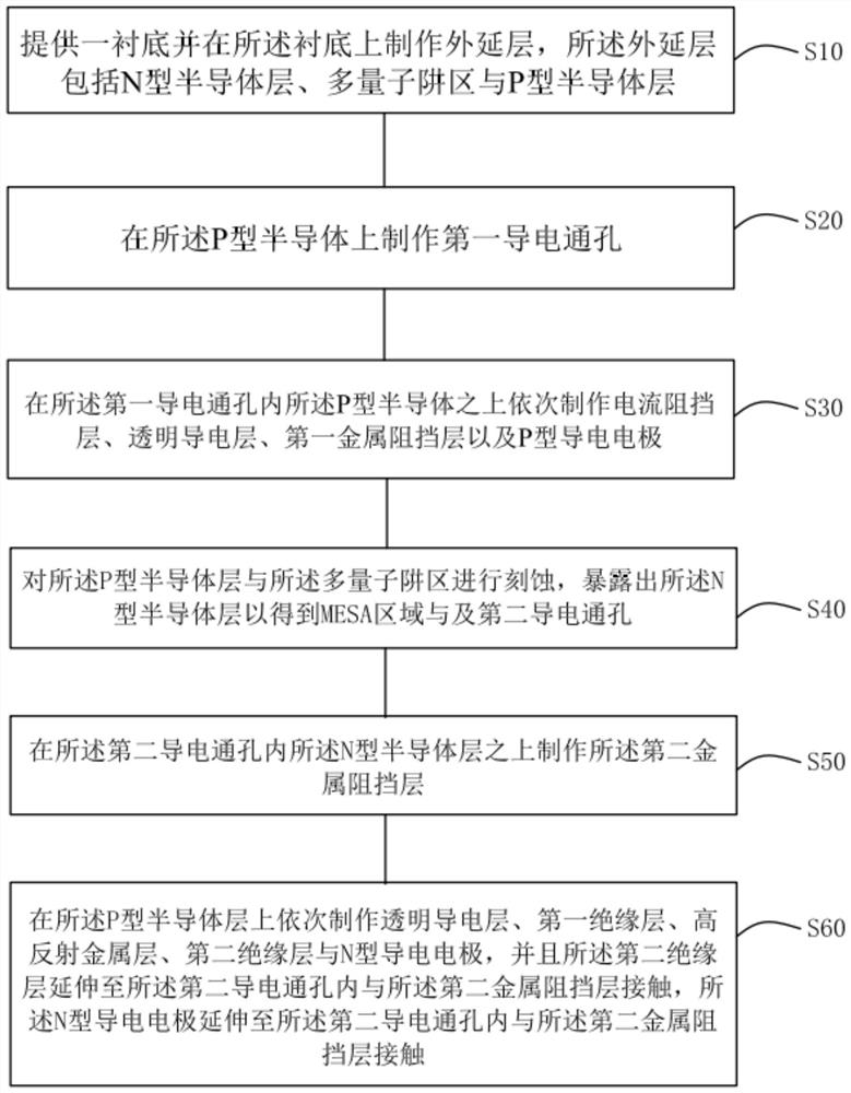
[0041] see figure 2 , the second embodiment of the present invention provides a preparation method of a high light efficiency LED chip, the preparation method is used to prepare the high light efficiency LED chip described in the first embodiment, and the preparation method includes steps S10-S60:

[0042] Step S10, providing a substrate and fabricating an epitaxial layer on the substrate, the epitaxial layer including an N-type semiconductor layer, a multiple quantum well region and a P-type semiconductor layer;

[0043] Step S20, forming a first conductive via on the P-type semiconductor;

[0044] Step S30, forming a current blocking layer, a transparent conductive layer, a first metal blocking layer and a P-type conductive electrode in sequence on the P-type semiconductor in the first conductive via;

[0045] Step S40, etching the P-type semiconductor layer and the multiple quantum well region to expose the N-type semiconductor layer to obtain a MESA region and a second c...


PUM


Abstract

The invention discloses a high-luminous-efficiency LED chip and a preparation method thereof. The chip comprises a substrate and an epitaxial layer, the current blocking layer is arranged on the P-type semiconductor layer; the transparent conducting layer is arranged on the current blocking layer; the first metal blocking layer and the second metal blocking layer are arranged on the transparent conducting layer; the first insulating layer is arranged on the transparent conducting layer; the high-reflection metal layer is arranged on the first insulating layer; the second insulating layer is arranged on the high-reflection metal layer; the high-reflection metal layer is insulated from the metal barrier layer; wherein the second insulating layer is provided with a P-type conductive electrode and an N-type conductive electrode, the P-type conductive electrode is in contact with the first metal barrier layer through a preset first conductive through hole so as to be connected with the P-type semiconductor layer, and the N-type conductive electrode is in contact with the second metal barrier layer through a preset second conductive through hole so as to be connected with the N-type semiconductor layer. The invention aims to improve the manufacturing process and ensure the production yield of the LED chip.

Description

technical field [0001] The invention relates to the technical field of light-emitting chips, in particular to a high-light-efficiency LED chip and a preparation method. Background technique [0002] A conventional blue-green LED chip generally includes a substrate, an epitaxial layer, a current blocking layer, a transparent conductive layer, a P-type electrode, an N-type electrode and an insulating protective layer. The epitaxial layer generally includes an N-type semiconductor, a multiple quantum well light-emitting region and a P-type electrode. The P-type electrode and the N-type electrode are electrically connected to the P-type semiconductor and the N-type semiconductor, respectively. Among them, the electrical connection between the N-type electrode and the N-type semiconductor needs to make MESA steps, that is, it is necessary to remove the P-type semiconductor and the multi-quantum well light-emitting region in the MESA step region. This process inevitably sacrifices...

Claims


Application Information

Patent Timeline
Patent Type & Authority Applications(China)
IPC IPC(8): H01L33/06H01L33/00H01L33/14H01L33/38
CPCH01L33/0062H01L33/06H01L33/145H01L33/38
Inventor 张星星张亚陈越简弘安胡加辉金从龙
Owner JIANGXI ZHAO CHI SEMICON CO LTD
Why Eureka
Try Eureka