Semiconductor workpiece double-sided detection device

A detection device, semiconductor technology, applied in the direction of comprehensive factory control, sorting, etc., can solve the problems of low use efficiency, automatic turning of workpieces, detection accuracy and efficiency reduction, etc., achieve a high degree of automation, improve detection accuracy, and facilitate operation. Effect

Pending Publication Date: 2022-07-08
领肯绳索科技江苏有限公司
View PDF9 Cites 1 Cited by
  • Summary
  • Abstract
  • Description
  • Claims
  • Application Information

AI Technical Summary

Problems solved by technology

[0002] With the diversification and complexity of semiconductor products and the improvement of product quality standards, the semiconductor packaging industry needs to monitor the quality of the product, check the appearance and size of the product and other parameters, and put the product on the tooling in related technologies , and then place it under X-rays to observe and measure the size of the product. Since the semiconductor product has two sides, one side of the semiconductor product is mounted with a chip, and the other side is not mounted with a chip, and the related design of the tooling can only check the mounting of the semiconductor product. On one side of the chip, the surface without the chip cannot be inspected, and the quality risk of the product cannot be monitored in time. In addition, in the prior art, the workpiece under inspection cannot be automatically turned over, resulting in a decrease in detection accuracy and efficiency. Therefore, a A device that can detect both sides of a semiconductor workpiece. The Chinese utility model patent with the publication number CN212721299U discloses a detection tool and a detection system. The detection tool is used for semiconductor workpiece detection. The detection tool includes a tool bracket and a baffle. The baffle plate is movably connected with the tooling bracket, and surrounds to form a placement groove, the placement groove is used to limit the workpiece, the baffle plate is used to adjust the size of the placement groove, and the bottom wall of the placement groove is set There is a way out
This prior art aims to provide a detection tool that is convenient for inspecting the surfaces on both sides of semiconductor workpieces. The detection tool effectively improves the product yield, and at the same time, it can realize adjustment and improve the versatility of the detection tool. However, this prior art still exists The following problems: (1) The semiconductor workpiece cannot be clamped and fixed; (2) It cannot be automatically turned over during the detection process, and the use efficiency is low. Therefore, the present invention provides a double-sided detection device for semiconductor workpieces, which can effectively solve the above-mentioned technologies question

Method used


Image

  • Semiconductor workpiece double-sided detection device
  • Semiconductor workpiece double-sided detection device
  • Semiconductor workpiece double-sided detection device

Examples


Embodiment

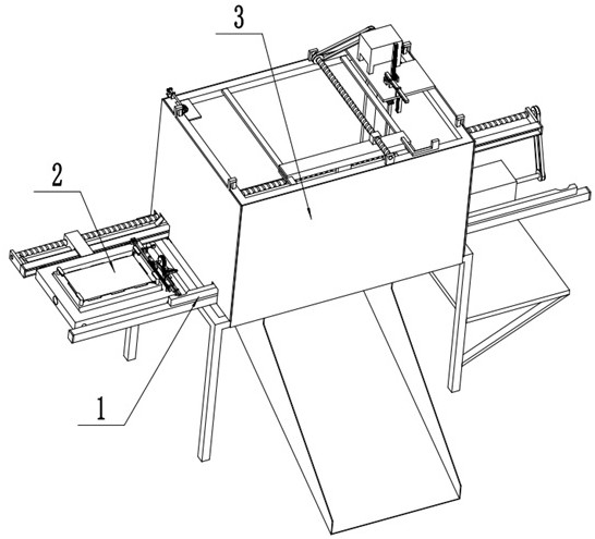
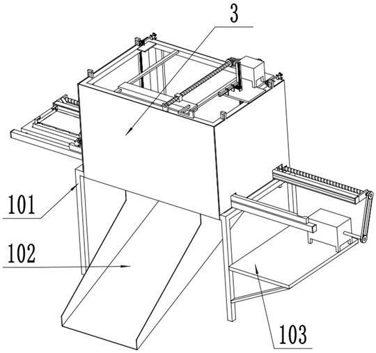
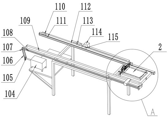
[0037] Example: as figure 1 , figure 2 , Figure 5 As shown, a double-sided detection device for a semiconductor workpiece includes a frame assembly 1, an installation assembly 2 and a detection assembly 3. The detection assembly 3 is arranged on the frame assembly 1, and the installation assembly 2 is slidably installed on the frame assembly 1. The assembly 2 is used to fix the semiconductor workpiece 4, and the mounting assembly 2 realizes the automatic clamping of the semiconductor workpiece 4 through the clamping drive assembly 206 and the clamping action assembly 208 during the sliding process of the mounting assembly 2 on the rack assembly 1. The mounting assembly 2 is mounted on the rack. During the sliding process of the assembly 1, the automatic turning is realized by the inversion driving assembly 207, and the double-sided detection of the semiconductor workpiece 4 is realized. automatically opens.

[0038] like figure 1 , figure 2 image 3 As shown, the fram...


PUM


Abstract

The invention discloses a semiconductor workpiece double-face detection device, and belongs to the technical field of semiconductor workpiece detection equipment, the semiconductor workpiece double-face detection device comprises a rack assembly, a mounting assembly and a detection assembly, the detection assembly is arranged on the rack assembly, the mounting assembly is slidably mounted on the rack assembly, and the mounting assembly is used for fixing a semiconductor workpiece; the mounting assembly automatically clamps a semiconductor workpiece through the clamping driving assembly in the sliding process of the mounting assembly on the rack assembly, the mounting assembly automatically turns over through the turning driving assembly in the sliding process of the mounting assembly on the rack assembly, double-face detection of the semiconductor workpiece is achieved, and a door opening assembly is arranged on the detection assembly. The door opening assembly is driven by the installation assembly to achieve automatic opening of the detection assembly. The device has the advantages of being high in automation degree, high in detection precision and convenient to operate.

Description

technical field [0001] The invention relates to the technical field of semiconductor workpiece detection equipment, in particular to a double-sided detection device for semiconductor workpieces. Background technique [0002] With the diversification and complexity of semiconductor products and the improvement of product quality standards, it is necessary to monitor the quality of the products in the process of the semiconductor packaging industry, and check the parameters such as the appearance and size of the products. In related technologies, the products need to be placed on the tooling. , and then placed under X-ray to observe and measure the product size. Since the semiconductor product has two sides, one side of the semiconductor product is mounted with a chip, and the other side is not mounted with a chip, and the related design tool can only check the mounting of the semiconductor product. On one side of the chip, the surface without the chip cannot be inspected, and...

Claims


Application Information

Patent Timeline
Patent Type & Authority Applications(China)
IPC IPC(8): B07C5/02
CPCB07C5/02Y02P90/02
Inventor 陈耀
Owner 领肯绳索科技江苏有限公司
Why Eureka
Try Eureka