Check patentability & draft patents in minutes with Patsnap Eureka AI!

Alignment mark structure, mask plate and semiconductor structure

A technology for aligning marks and semiconductors, applied in semiconductor devices, semiconductor/solid-state device components, electric solid-state devices, etc., can solve problems affecting bonding quality, affecting chemical-mechanical flatness, introducing too many bubbles, etc., to achieve improvement The effect of bonding quality, reducing the burden of etching, and meeting size requirements

Pending Publication Date: 2022-07-15
YANGTZE MEMORY TECH CO LTD
View PDF0 Cites 0 Cited by
  • Summary
  • Abstract
  • Description
  • Claims
  • Application Information

AI Technical Summary

Problems solved by technology

However, in some specific usage scenarios, when some grating marks are not used for photolithography alignment, these grating marks are likely to introduce too many air bubbles during the bonding process, thereby affecting the bonding quality; at the same time, it is easy to affect the chemical mechanical planarization process. flatness of

Method used


Image

  • Alignment mark structure, mask plate and semiconductor structure
  • Alignment mark structure, mask plate and semiconductor structure
  • Alignment mark structure, mask plate and semiconductor structure

Examples


Embodiment Construction

[0031] In order to make the objectives, technical solutions and advantages of the present invention clearer, the present invention will be further described in detail below with reference to the accompanying drawings and embodiments. It should be understood that the specific embodiments described herein are only used to explain the present invention, but not to limit the present invention.

[0032] In the description of the present invention, the terms "inner", "outer", "longitudinal", "lateral", "top", "bottom", "top", "bottom", "left", "right", "front" ”, “rear”, etc. are based on the orientation or positional relationship shown in the drawings, and are only for the convenience of describing the present invention rather than requiring the present invention to be constructed and operated in a specific orientation, and therefore should not be construed as Limitations of the present invention.

[0033] In the description of the present invention, when an element or layer is re...


PUM

PropertyMeasurementUnit
Widthaaaaaaaaaa

Abstract

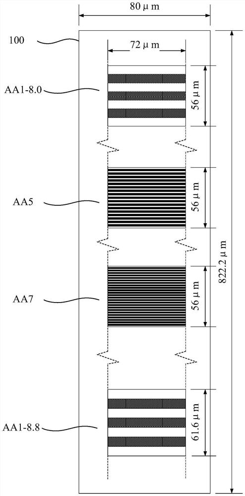
The embodiment of the invention discloses an alignment mark structure for photoetching equipment, a mask plate and a semiconductor structure. The alignment mark structure comprises a plurality of main marks and is used for realizing alignment in a photoetching process; each main mark in the plurality of main marks comprises a plurality of alignment grid bars which are parallel to one another and are arranged at intervals; the dummy mark is used for matching the size requirement of the photoetching equipment; and the dummy mark comprises a plurality of dot-shaped structures which are arranged at intervals in an array.

Description

technical field [0001] The present invention relates to the technical field of semiconductors, and in particular, to an alignment mark structure for a lithography apparatus, a mask plate and a semiconductor structure including the same. Background technique [0002] In the field of semiconductor lithography, a scribe groove alignment method is a widely used alignment method in current lithography technology. Scribing trenches, also known as scribe lanes, are used for dicing to cut a wafer into multiple dies (or dies). Alignment marks, such as long and narrow rectangular scribe lane primary marks (SPM), are formed in the scribe lanes of each layer or layers, and the alignment marks in the latter layer may be the same as those in the previous layer or layers. Alignment marks in the layers are aligned. [0003] In the related art, a scribing groove main mark with high precision is provided, and the large-sized scribing groove main mark has the advantages of wide capture range...

Claims


Application Information

Patent Timeline
IPC IPC(8): G03F9/00G03F1/76H01L23/544
CPCG03F9/708G03F9/7076G03F1/76H01L23/544H01L2223/54426
Inventor 胡帅张鹏真徐陈林彭熙锦王梦婷崔佳森
Owner YANGTZE MEMORY TECH CO LTD
Features
  • R&D
  • Intellectual Property
  • Life Sciences
  • Materials
  • Tech Scout
  • Unparalleled Data Quality
  • Higher Quality Content
  • 60% Fewer Hallucinations
Learn More