Wafer clamping device
A clamping device and wafer technology, which is applied in the manufacture of electrical components, circuits, semiconductors/solid-state devices, etc., can solve the problems of poor compatibility of wafer clamping devices, and achieve good adaptability, easy adjustment, and shortened distances.
- Summary
- Abstract
- Description
- Claims
- Application Information
AI Technical Summary
Problems solved by technology
Method used
Image

Examples
Embodiment 1
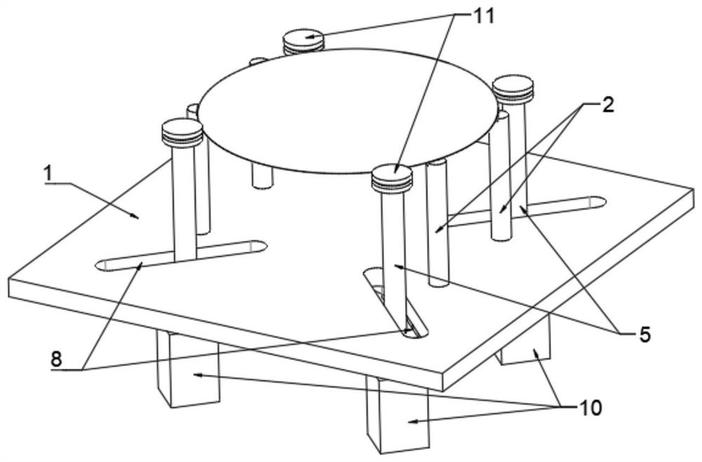
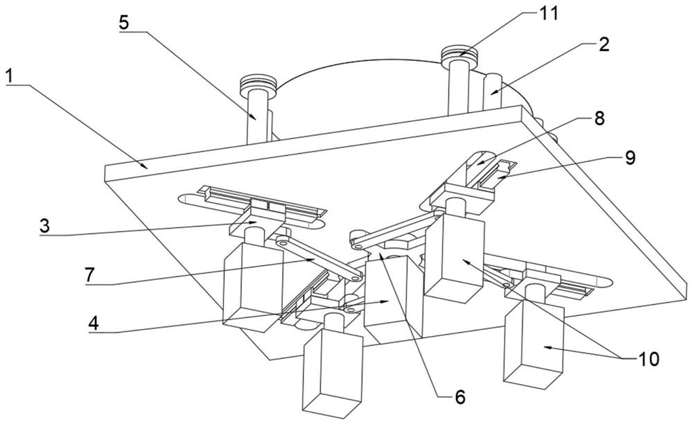
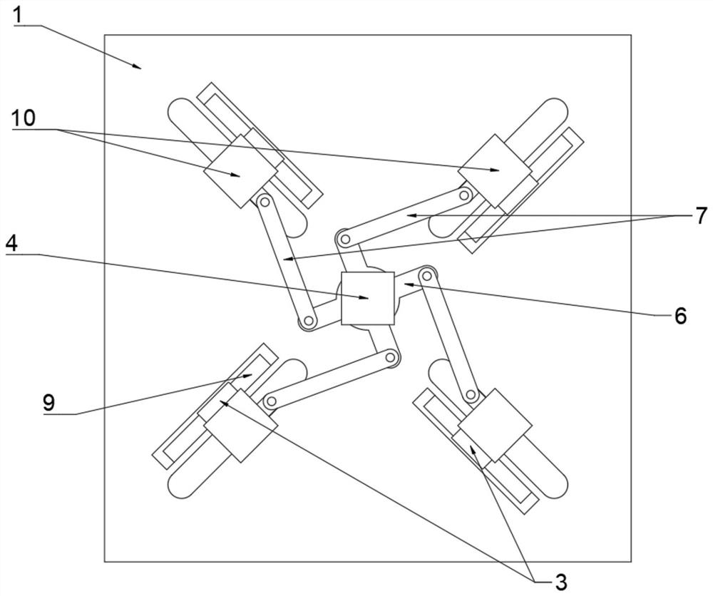
[0037] combine Figure 1-Figure 3 As shown, the wafer clamping device provided in this embodiment includes: a base plate 1; at least two support columns 2, both of which are arranged on the upper surface of the base plate 1 and are suitable for supporting wafers; a plurality of sliders 3, based on the base plate 1. The center of a virtual circle in the plane is symmetrically distributed in the center. Each slider 3 is slidably installed on the base plate 1, and the sliding direction is consistent with the radial direction of the virtual circle. The slider 3 is connected with a radial direction that drives it along the virtual circle. The sliding first driving member 4, the first driving member 4 can continuously adjust the position of the sliding block 3 in the radial direction of the virtual circle; a plurality of clamping shafts 5 correspond to the sliding block 3 one by one, and are installed on the sliding block 3, The top side of the clamping shaft 5 is adapted to contact...
PUM
 Abstract
Description
Claims
Application Information