Chip and wafer cutting method for improving silver colloid climbing in welding process

A technology of welding process and cutting method, which is applied in the direction of semiconductor/solid-state device parts, semiconductor devices, electrical components, etc., can solve the problems of high product scrap rate, reduce scrap rate, improve silver glue climbing, and improve product reliability and economical effects

Pending Publication Date: 2022-07-22
重庆万国半导体科技有限公司
View PDF0 Cites 0 Cited by
  • Summary
  • Abstract
  • Description
  • Claims
  • Application Information

AI Technical Summary

Problems solved by technology

[0006] In order to improve the problem of high product scrap rate caused by partial silver glue climbing and improve product reliability, the present invention provides a wafer cutting method for improving silver glue climbing during chip welding

Method used


Image

  • Chip and wafer cutting method for improving silver colloid climbing in welding process
  • Chip and wafer cutting method for improving silver colloid climbing in welding process
  • Chip and wafer cutting method for improving silver colloid climbing in welding process

Examples


Embodiment 1

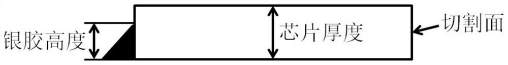
[0050] A wafer cutting method for improving the climbing of silver glue during chip welding, comprising the following steps:

[0051] Step S1, wafer cutting preparation: after receiving the wafer to be cut, first check whether there is a film on the back of the incoming wafer. If there is no film, a film needs to be applied to the back of the wafer. If there is a film, you need to check whether the back film has expired. If the film on the back has expired, it will need to be replaced with an unexpired film.

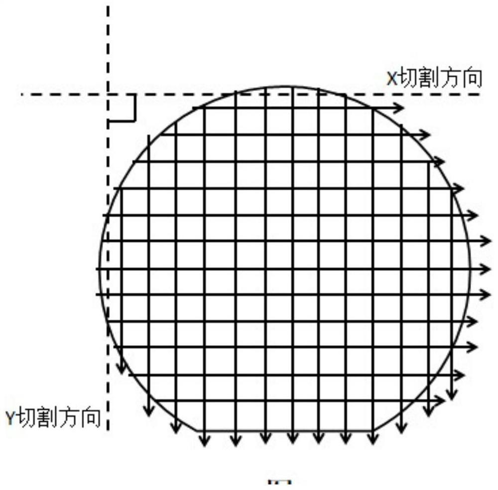
[0052] Step S2, wafer cutting: combining figure 1 As shown, when a wafer is prepared for various cutting tasks, the blade 1 with a wider knife mark is selected, which is used for the initial cutting of each cutting line of the wafer. The width of the knife mark is W1, the cutting thickness is set to Z1, and then the grooving cutting of each dicing lane in the X direction is started.

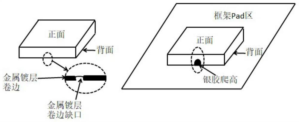
[0053] When the blade 1 steps to the Nth cutting lane in the X direction, the syste...

Embodiment 2

[0068] A wafer cutting method for improving the climbing of silver glue during chip welding, comprising the following steps:

[0069] Step S1, wafer cutting preparation: After receiving the wafer to be cut, first check whether there is a film on the back of the incoming wafer. If there is no film, the film needs to be applied to the back of the wafer. If there is a film, you need to check whether the back film has expired. If the film on the back has expired, it will need to be replaced with an unexpired film.

[0070] Step S2, wafer cutting: combining figure 1 As shown, when a wafer is prepared for various cutting tasks, the blade 1 with a wider knife mark is selected, which is used for the initial cutting of each cutting line of the wafer. The width of the knife mark is W1, the cutting thickness is set to Z1, and then the grooving cutting of each cutting lane in the X direction is started.

[0071] When the blade 1 steps to the Nth cutting lane in the X direction, the sy...

Embodiment 3

[0086] A wafer cutting method for improving the climbing of silver glue during chip welding, comprising the following steps:

[0087] Step S1, wafer cutting preparation: After receiving the wafer to be cut, first check whether there is a film on the back of the incoming wafer. If there is no film, the film needs to be applied to the back of the wafer. If there is a film, you need to check whether the back film has expired. If the film on the back has expired, it will need to be replaced with an unexpired film.

[0088] Step S2, wafer cutting: combining figure 1 As shown, when a wafer is prepared for various cutting tasks, the blade 1 with a wider knife mark is selected, which is used for the initial cutting of each cutting line of the wafer. The width of the knife mark is W1, the cutting thickness is set to Z1, and then the grooving cutting of each cutting lane in the X direction is started.

[0089] When the blade 1 steps to the Nth cutting lane in the X direction, the sy...


PUM

PropertyMeasurementUnit
thicknessaaaaaaaaaa

Abstract

The invention discloses a chip for improving silver colloid climbing in a welding process and a wafer cutting method, the peripheral side of the chip is provided with step-shaped anti-colloid-climbing convex blocks, the number of the anti-colloid-climbing convex blocks is greater than or equal to 1, the total height of the anti-colloid-climbing convex blocks is Z2, the distance between one side, close to the upper surface of the chip, of each anti-colloid-climbing convex block and the upper surface of the chip is Z1, and Z2 is greater than Z3. The thickness of the chip is the sum of Z1 and Z2; the ratio of Z2 to the sum of Z1 and Z2 is A, and the value range of A is 10%-90%. The cutting method comprises the following steps of S1, wafer cutting preparation; step S2, cutting the wafer; cutting each cutting channel of the wafer through a plurality of blades, wherein the cutting frequency is greater than or equal to 2 times; and S3, the climbing height of the silver colloid or soldering paste chip mounting local welding material is smaller than 90% of the height of the chip, the scrap rate of the chip cut through the wafer cutting method is reduced to 0% from 3.5%, and the product reliability and economic benefits are greatly improved.

Description

technical field [0001] The invention relates to the field of wafer cutting, in particular to a chip and a wafer cutting method for improving the climbing of silver glue during welding. Background technique [0002] Silicon-based wafer dicing is currently a relatively mature technology. Usually, the wafer is pasted and fixed before the wafer is cut, and then the size and thickness of the wafer are measured, and finally the appropriate blade is selected to cut the wafer. [0003] like figure 1 As shown, the wafer is generally cut based on the same X direction first, and then the wafer is cut based on the Y direction perpendicular to the X direction. For an ordinary single chip, a relatively flat or slightly uneven shape will be formed around the chip after cutting. like figure 2 As shown, in general, even if it is cut multiple times, it will try to make the cutting surface of the side of the chip become a flat plane. [0004] process as image 3 As shown, in the current...

Claims


Application Information

Patent Timeline
Patent Type & Authority Applications(China)
IPC IPC(8): H01L23/488H01L23/00H01L21/78
CPCH01L23/488H01L23/564H01L21/78
Inventor 陈建华汪利民瞿伟胡杰黄鑫
Owner 重庆万国半导体科技有限公司
Why Eureka
Try Eureka