
Circuit board defect testing method

A defect testing and circuit board technology, applied in the field of circuit board analysis, which can solve problems such as poor soldering quality of solder joints and cracking of solder joints

Pending Publication Date: 2022-07-29
CHINA ELECTRONICS PROD RELIABILITY & ENVIRONMENTAL TESTING RES INST
View PDF1 Cites 0 Cited by
  • Summary
  • Abstract
  • Description
  • Claims
  • Application Information

AI Technical Summary

Problems solved by technology

Since the solder joints will be separated prior to the cracks when they are separated by mechanical stress, after the solder joints are pulled out, if there is red pigment remaining on the separation surface of the solder joints, it means that there are cracks in the solder joints and the welding quality of the solder joints is not good.
Although this test method can be used to detect the soldering quality of the solder joints on the circuit board, it needs to split the original sample by pulling out during the detection process for subsequent observations, so it can only be applied to such as solder joints. and other easily separable parts

Method used


Image

  • Circuit board defect testing method
  • Circuit board defect testing method

Examples


Embodiment 1

[0057] Immerse the part to be tested on the circuit board in a fluorescent penetrant solution, the fluorescent penetrant solution includes a fluorescent penetrant and an organic solvent, and the mass ratio of the fluorescent penetrant and the organic solvent is 1:20. The fluorescent osmotic solution selected from the new Mita CY-3800 fluorescent osmotic fluid, other fluorescent osmotic fluids can also play a similar role.

[0058] Put the circuit board and the fluorescent osmotic solution together in the vacuum chamber, firstly evacuating the vacuum chamber until the vacuum degree is reduced to below -0.1MPa, keep the vacuum chamber for 3min, return the vacuum chamber to normal pressure, and repeat the vacuuming and Steps to return to normal pressure twice.

[0059] The circuit board was taken out from the fluorescent permeation solution and placed in an oven, the temperature of the oven was 80° C., and the baking time was 1 h, so that there was no residual fluorescent permeat...

Embodiment 2

[0063] Immerse the part to be tested on the circuit board in a fluorescent penetrant solution, the fluorescent penetrant solution includes a fluorescent penetrant and an organic solvent, and the mass ratio of the fluorescent penetrant and the organic solvent is 1:20.

[0064] The circuit board and the fluorescent penetrating solution are placed in a vacuum chamber together, and the vacuum chamber is first evacuated until the vacuum degree is reduced to below -0.1MPa, and kept for 10min.

[0065] The circuit board was taken out from the fluorescent permeation solution and placed in an oven, the temperature of the oven was 80° C., and the baking time was 1 h, so that there was no residual fluorescent permeation solution on the circuit board.

[0066] The circuit board is sampled to obtain the sample to be tested, the sample to be tested is sealed with epoxy resin, and then the sample to be tested is sliced ​​to expose the observation section to be observed, and after slicing, it ...

Embodiment 3

[0069] Immerse the part to be tested on the circuit board in a fluorescent penetrant solution, the fluorescent penetrant solution includes a fluorescent penetrant and an organic solvent, and the mass ratio of the fluorescent penetrant and the organic solvent is 1:30.

[0070] The circuit board and the fluorescent penetrating solution are placed in a vacuum chamber together, and the vacuum chamber is first evacuated until the vacuum degree is reduced to below -0.1MPa, and kept for 10min.

[0071] The circuit board was taken out from the fluorescent permeation solution and placed in an oven, the temperature of the oven was 80° C., and the baking time was 1 h, so that there was no residual fluorescent permeation solution on the circuit board.

[0072] The circuit board is sampled to obtain the sample to be tested, the sample to be tested is sealed with epoxy resin, and then the sample to be tested is sliced ​​to expose the observation section to be observed, and after slicing, it ...


PUM


Abstract

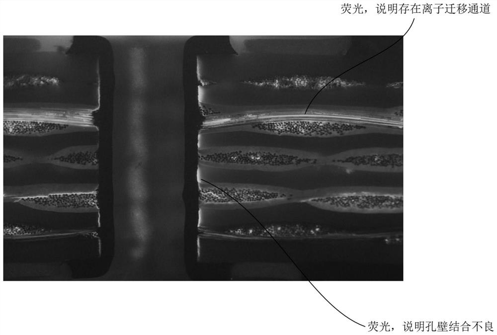
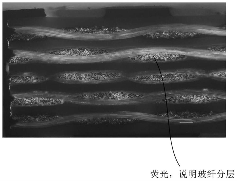
The invention provides a circuit board defect testing method, which comprises the following steps: a to-be-tested part on a circuit board is immersed in a fluorescent penetration solution, the fluorescent penetration solution comprises a fluorescent penetrant and an organic solvent, and the mass ratio of the fluorescent penetrant to the organic solvent is 1: (20-30); placing the circuit board and the fluorescent penetrating solution in a vacuum chamber together, and vacuumizing the vacuum chamber; and taking out the circuit board, removing the residual fluorescent penetrating solution on the circuit board, slicing the circuit board to expose the observation cross section, and detecting the fluorescent effect of the observation cross section. The circuit board defect testing method can be used for testing various structural defects on the circuit board, observation can be carried out only by cutting out a small number of circuit board samples and making the circuit board samples into slices, and the required inspection instrument is simple, low in cost and fast in time efficiency.

Description

technical field [0001] The invention relates to the technical field of circuit board analysis, in particular to a circuit board defect testing method. Background technique [0002] As the main development direction of the new generation of mobile communication technology, 5G communication has three basic performance requirements: full spectrum access, high frequency band and even millimeter wave transmission, and high spectrum efficiency. In the development of communications in recent years, its base stations are all over the world, and the operating environment ranges from high temperature and high humidity in the equator to severe cold areas in the extreme north. The harsh environment also puts forward higher performance and upgrade requirements for devices and raw materials. . [0003] Among all kinds of device raw materials used in base stations, printed circuit boards play an important role in receiving devices, transmitting power signals, and supporting circuits. The...

Claims


Application Information

Patent Timeline
IPC IPC(8): G01N21/91
CPCG01N21/91
Inventor 洪瑛旭陈泽坚何骁邹雅冰杨颖周亮沈江华朱海泉
Owner CHINA ELECTRONICS PROD RELIABILITY & ENVIRONMENTAL TESTING RES INST
Learn More