
Virtual inking method for wafer

A wafer and wafer testing technology, applied in the field of integrated circuit manufacturing, can solve the problems of poor ink printing accuracy, error-prone, low efficiency, etc., and achieve the effects of improving efficiency, avoiding differences and misoperations, and unifying rules

Pending Publication Date: 2022-07-29
厦门士兰集科微电子有限公司
View PDF0 Cites 0 Cited by
  • Summary
  • Abstract
  • Description
  • Claims
  • Application Information

AI Technical Summary

Problems solved by technology

[0005] The purpose of the present invention is to provide a method for virtual inking of wafers to solve the problems of poor accuracy, low efficiency, and error-prone in the existing manual virtual inking.

Method used

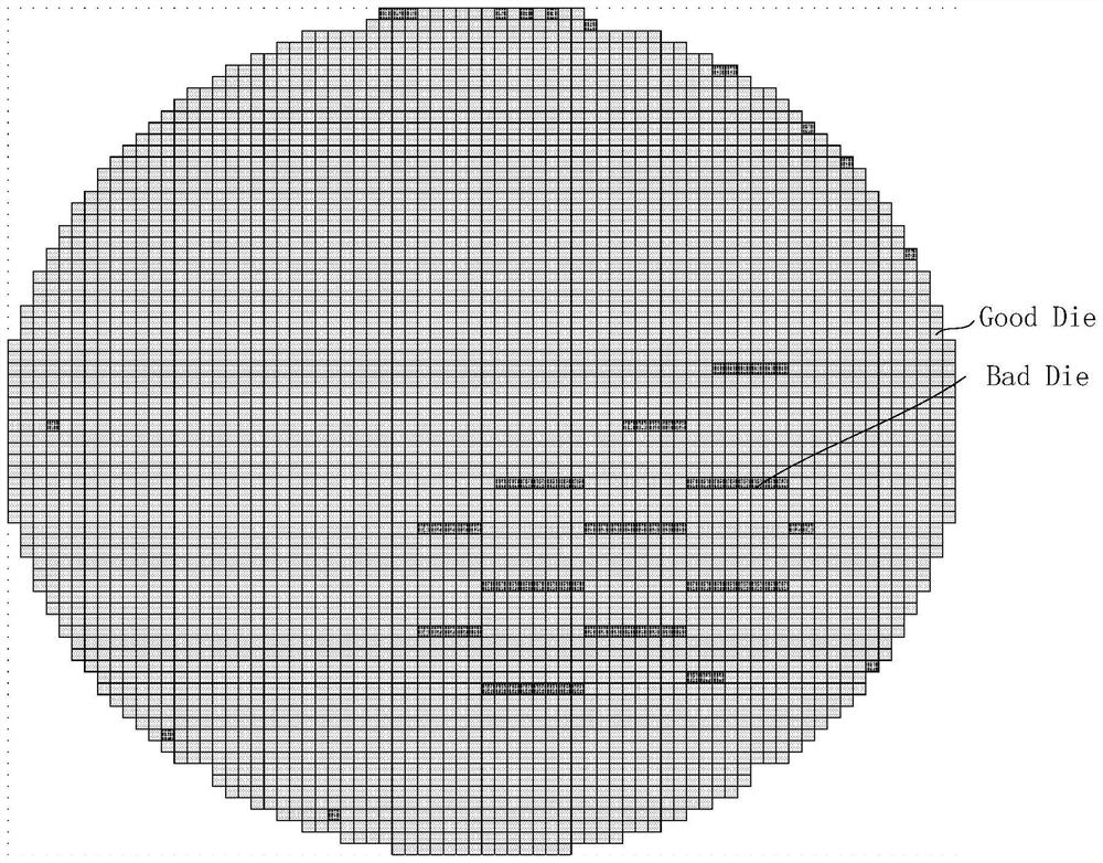
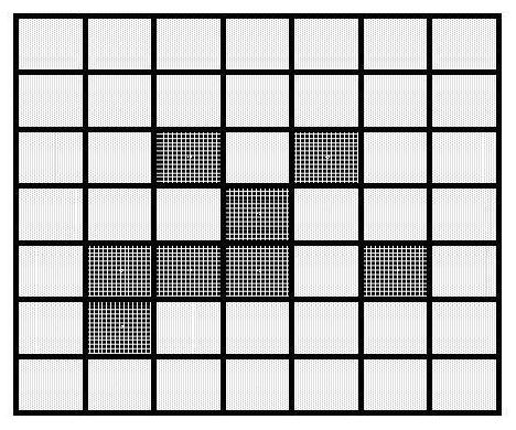

Image

  • Virtual inking method for wafer
  • Virtual inking method for wafer
  • Virtual inking method for wafer

Examples


Embodiment Construction

[0042] The specific embodiments of the present invention will be described in more detail below with reference to the schematic diagrams. The advantages and features of the present invention will become more apparent from the following description. It should be noted that, the accompanying drawings are all in a very simplified form and in inaccurate scales, and are only used to facilitate and clearly assist the purpose of explaining the embodiments of the present invention.

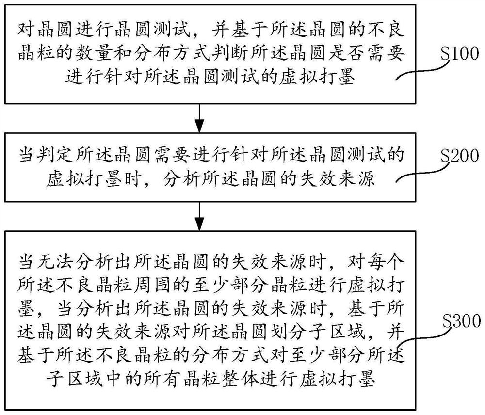
[0043] figure 1 This is a flowchart of the method for virtual inking of wafers provided in this embodiment. like figure 1 As shown, the virtual inking method for a wafer provided by this embodiment includes step S100, step S200 and step S300.

[0044]Step S100 is performed to perform a wafer test on the wafer, and based on the number and distribution of defective die of the wafer, it is determined whether the wafer needs to be subjected to virtual inking for the wafer test.

[0045] in particular, f...


PUM


Abstract

The invention provides a virtual inking method for a wafer, which comprises the following steps of: firstly, judging whether the wafer needs to be subjected to virtual inking aiming at a wafer test or not based on the number and the distribution mode of bad crystal grains of the wafer, if so, analyzing a failure source of the wafer, and if the failure source of the wafer cannot be analyzed, judging whether the wafer needs to be subjected to virtual inking aiming at the wafer test; and performing virtual inking on at least part of the crystal grains around each bad crystal grain, when the failure source of the wafer is analyzed, dividing the wafer into sub-regions based on the failure source of the wafer, and performing virtual inking on all the crystal grains in at least part of the sub-regions based on the distribution mode of the bad crystal grains. According to the method, manual participation is not needed, the virtual ink printing rule is uniform, the difference and misoperation of manual operation are avoided, and the virtual ink printing efficiency is improved.

Description

technical field [0001] The present invention relates to the technical field of integrated circuit manufacturing, in particular to a method for virtual inking of wafers. Background technique [0002] Generally, the integrated circuit manufacturing process can be divided into the wafer manufacturing stage, the chip testing stage and the chip packaging stage in sequence. As the current electronic products pay attention to lightness, thinness and shortness, the packaging technology at this stage has been gradually reduced in order to reduce the package volume and improve the performance of the integrated circuit. Tends to high-end packaging technologies such as flip-chip packaging and multi-chip modules. However, these high-end packaging methods are expensive, so it is best to perform wafer testing (CP testing) on ​​wafers before packaging, so as to be packaged in the later stage. Defective dies on the wafer are removed before the process, saving unnecessary packaging costs. ...

Claims


Application Information

Patent Timeline
Patent Type & Authority Applications(China)
IPC IPC(8): G01R31/28
CPCG01R31/2851
Inventor 罗莹莹陈燕华骆向荣徐亚楠王淋雨李文博张亮
Owner 厦门士兰集科微电子有限公司
Learn More