Method and device for measuring semiconductor multilayer structure based on second harmonic

A second harmonic, multi-layer structure technology, applied in the direction of semiconductor/solid-state device testing/measurement, etc., can solve the problem of result error, difficult to unify, unable to measure the whole area of ​​the wafer, etc., to achieve the effect of improving the measurement accuracy

Active Publication Date: 2022-07-29
SHANGHAI ASPIRING SEMICON EQUIP CO LTD
View PDF7 Cites 0 Cited by
  • Summary
  • Abstract
  • Description
  • Claims
  • Application Information

AI Technical Summary

Problems solved by technology

[0005]1) In the existing measurement technology, it is difficult to unify the actual measurement results with the theoretical model, which makes it impossible to decouple the various factors that generate the second harmonic, which It is also the main reason why this technology is currently only used as a qualitative analysis method rather than a quantitative analysis method.
[0006]2) Existing technologies or theoretical models cannot perform global measurement on wafers under the premise of ensuring high measurement efficiency
[0007]3) The accuracy of the existing second harmonic detection equipment is not enough, especially the measurement accuracy of the initial value of one of the most important parameters is not enough, which leads to the Values ​​will cause errors in the results when analyzing sample parameters

Method used


Image

  • Method and device for measuring semiconductor multilayer structure based on second harmonic
  • Method and device for measuring semiconductor multilayer structure based on second harmonic
  • Method and device for measuring semiconductor multilayer structure based on second harmonic

Examples


Embodiment Construction

[0070] specific implementation

[0071] The term "and / or" in this article is only an association relationship to describe the associated objects, indicating that there can be three kinds of relationships, for example, A and / or B, it can mean that A exists alone, A and B exist at the same time, and A and B exist independently B these three cases.

[0072] The technical solutions in the embodiments of the present application will be clearly and completely described below with reference to the accompanying drawings in the embodiments of the present application. It should be understood by those skilled in the art that the described embodiments are some, but not all, embodiments of the present invention. Based on the embodiments in this application, those skilled in the art can make any suitable modifications or variations to obtain all other embodiments.

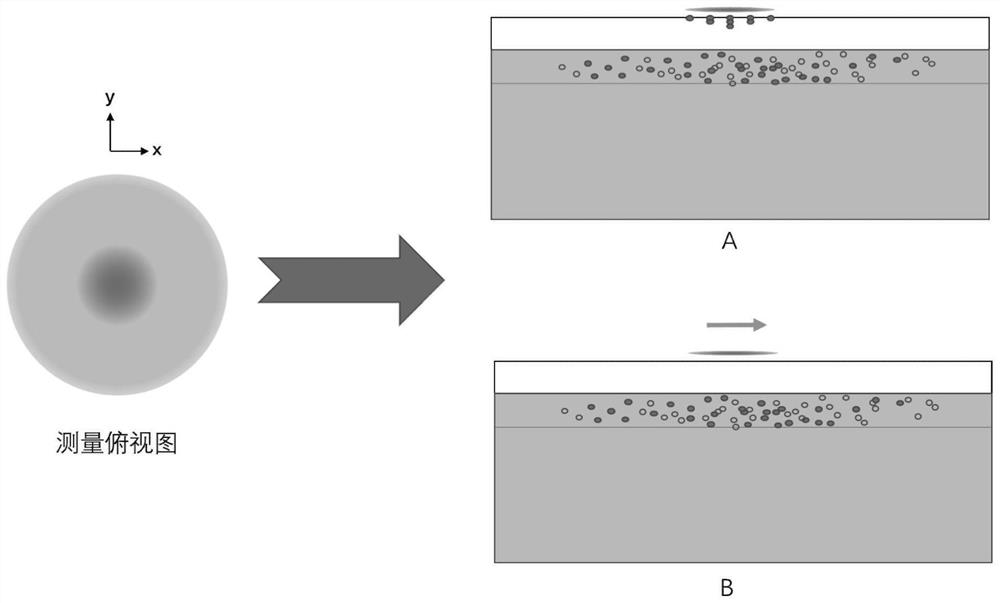
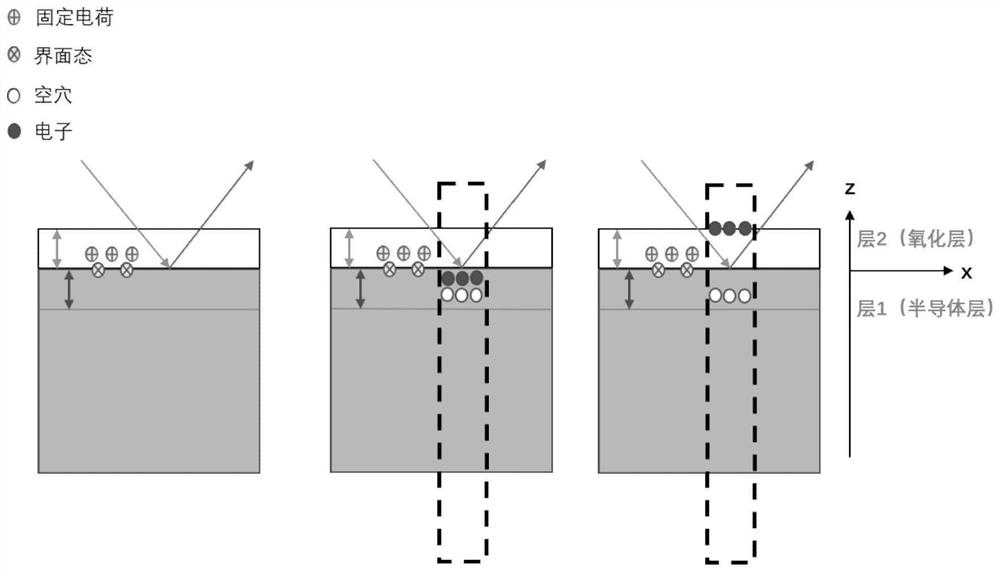
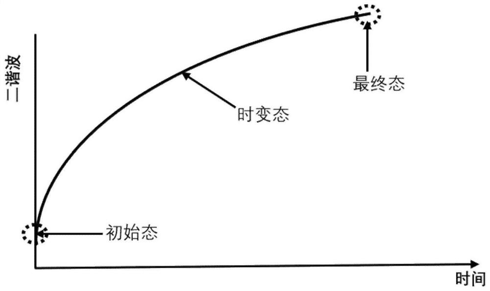
[0073] In a first aspect, an embodiment of the present invention provides a method for measuring a semiconductor multilayer ...


PUM


Abstract

The invention provides a two-harmonic-wave-based measurement method and device for wafer global measurement. The scheme comprises three modes of fixed-point measurement, scanning measurement and combination of fixed-point measurement and scanning measurement. According to the scanning measurement scheme, global measurement can be carried out on the wafer on the premise that high measurement efficiency is guaranteed, the position, size and relative density distribution of electrical defects are obtained, and positioning and troubleshooting of wafer abnormal points are achieved, which cannot be achieved through a previous two-harmonic measurement technology. The invention also provides a novel formula system for describing the second harmonic signal, so that the actual measurement result and the theoretical model are unified under the three conditions of fixed-point measurement, scanning measurement and combination of fixed-point measurement and scanning measurement, the second harmonic measurement technology is not only a qualitative analysis method any more, and the measurement accuracy is improved. And the method can be applied as a quantitative analysis method, so that the comprehensiveness and the accuracy of product detection are improved on the premise of ensuring the efficiency, and the quality inspection capability in the advanced manufacturing process of the semiconductor is improved.

Description

technical field [0001] The invention relates to the measurement of a semiconductor device in the process of manufacturing or processing, mainly measuring or monitoring the interface characteristics or the quality of the oxide layer of the semiconductor wafer through the second harmonic wave. Background technique [0002] Quality inspection at the interface between oxide and semiconductor layers has always been an important part of semiconductor wafer processing. This is because the interfacial state and the bulk charge of the oxide layer existing at the interface will cause the device threshold voltage instability and leakage by trapping or releasing carriers, which greatly reduces the performance and service life of the device. [0003] At present, the main methods commonly used in the industry to quantitatively characterize such electrical properties are the conductance method and the capacitance method. The principle is that although such electrical characteristics will ...

Claims


Application Information

Patent Timeline
Patent Type & Authority Applications(China)
IPC IPC(8): H01L21/66
CPCH01L22/12H01L22/20
Inventor 黄崇基赵威威周朴希
Owner SHANGHAI ASPIRING SEMICON EQUIP CO LTD
Why Eureka
Try Eureka