High dielectric constant metal gate MOS transistor

A MOS transistor, high dielectric constant technology, applied in transistors, circuits, electrical components, etc., can solve the problems of N-type metal work function layer work function shift, diffusion, NMOS threshold voltage shift, etc., to prevent drift , reduce threshold voltage fluctuations, and improve stability

Pending Publication Date: 2022-07-29
SHANGHAI HUALI INTEGRATED CIRCUTE MFG CO LTD
View PDF0 Cites 2 Cited by
  • Summary
  • Abstract
  • Description
  • Claims
  • Application Information

AI Technical Summary

Problems solved by technology

like figure 2 As mentioned above, the top capping layer 107 has a columnar polycrystalline structure, and there are grain boundaries 201 between each column, and the grain boundaries 201 will form an oxygen diffusion path, and finally cause oxygen diffusion as shown by the mark 202, O 2 After diffusion to the surface of the TiAl layer 106, the TiAl layer 106 will be oxidized to form a TiAl oxide layer 203. The oxide layer 203 includes aluminum oxide. Finally, the actual N-type metal work function layer is formed by stacking the TiAl layer 106 and the oxide layer 203. As a result, since the work function of the oxide layer 203 is different from the work function of the TiAl layer 106, the work function of the N-type metal work function layer will eventually shift, and finally the threshold voltage of the NMOS will also shift.

Method used


Image

  • High dielectric constant metal gate MOS transistor
  • High dielectric constant metal gate MOS transistor
  • High dielectric constant metal gate MOS transistor

Examples


Embodiment Construction

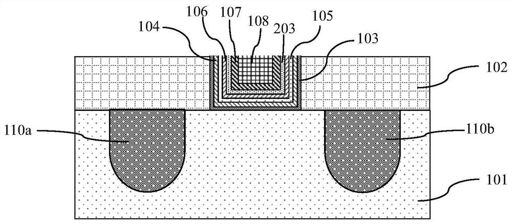
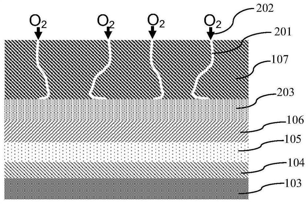
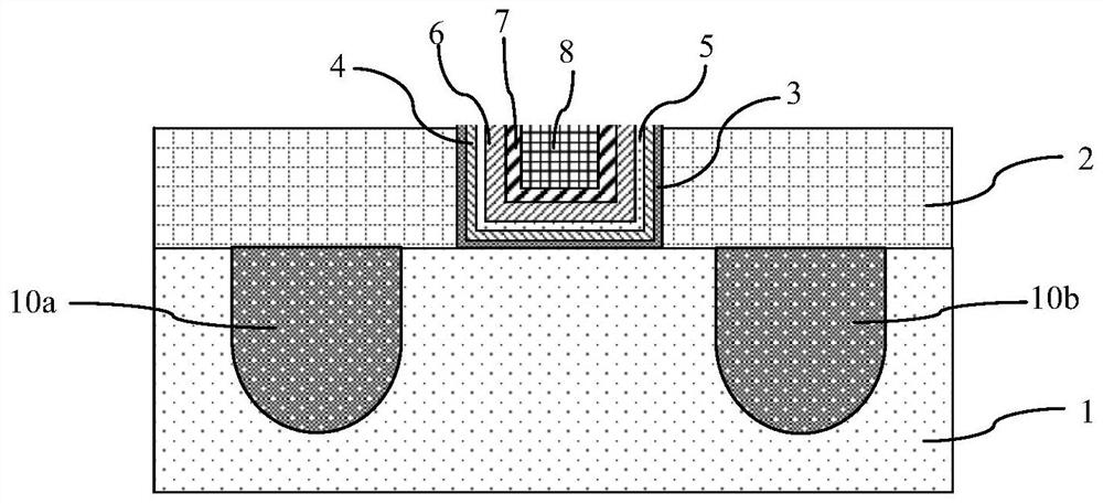
[0049] like image 3 shown is a schematic cross-sectional structure diagram of a high dielectric constant metal gate MOS transistor along the channel length direction according to an embodiment of the present invention, image 3 The high-k metal-gate MOS transistors shown in are NMOS; as Figure 4 shown is a schematic cross-sectional structure diagram of a high dielectric constant metal gate MOS transistor along the channel width direction according to an embodiment of the present invention; Figure 5 shown, yes image 3 The schematic diagram of the elimination oxygen diffusion path formed by the top cap layer 7 of the high dielectric constant metal gate MOS transistor in the embodiment of the present invention is shown; taking NMOS as an example, the high dielectric constant of the high dielectric constant metal gate MOS transistor in the A constant metal gate is formed on the semiconductor substrate 401 .

[0050] The high dielectric constant metal gate includes: a gate d...


PUM


Abstract

The invention discloses a high-dielectric-constant metal gate MOS (Metal Oxide Semiconductor) transistor. A high-dielectric-constant metal gate comprises a gate dielectric layer, a metal work function layer, a top cap layer and a metal conductive material layer, the gate dielectric layer comprises a high dielectric constant layer; the metal work function layer is located at the top of the gate dielectric layer; the top cap layer is located between the metal work function layer and the metal conductive material layer, the top cap layer adopts a material capable of preventing metal of the metal conductive material layer from diffusing to the bottom into the metal work function layer and adopts an amorphous structure, so that oxygen diffusion paths are reduced or eliminated, and oxidation of the surface of the metal work function layer is reduced or eliminated. According to the invention, the top surface of the metal work function layer can be prevented from being oxidized, so that the work function is prevented from deviating, and the threshold voltage of the device is prevented from drifting.

Description

technical field [0001] The present invention relates to a semiconductor integrated circuit, in particular to a high dielectric constant metal gate (HKMG) MOS transistor. Background technique [0002] With the development of CMOS technology, traditional silicon dioxide gate dielectric and polysilicon gate (Poly SiON) transistors have reached physical limits, such as the problem of excessive leakage current due to quantum tunneling effect and the depletion of polysilicon gate. Problems and the like seriously affect the performance of semiconductor devices. Starting from the 45nm technology node, the HKMG stack transistor developed on the basis of the HKMG process effectively solves the above technical problems. [0003] The gate structure of the high dielectric constant metal gate MOS transistor adopts HKMG, and HKMG includes a high dielectric constant layer (HK) and a metal gate (MG), wherein the metal gate includes a metal work function layer and a metal conductive material...

Claims


Application Information

Patent Timeline
Patent Type & Authority Applications(China)
IPC IPC(8): H01L29/78H01L29/49
CPCH01L29/785H01L29/4966H01L29/513H01L29/66545H01L21/28088H01L29/42364H01L29/42372H01L27/092
Inventor 魏程昶苏炳熏何德彪吴方锐
Owner SHANGHAI HUALI INTEGRATED CIRCUTE MFG CO LTD
Why Eureka
Try Eureka