Contact hole etching method of CMOS device and CMOS device manufacturing method

A contact hole etching and contact hole technology, which is applied in semiconductor/solid-state device manufacturing, semiconductor devices, electrical components, etc., can solve the problems of device cost increase, save manufacturing steps, avoid insufficient etching, and avoid over-etching The effect of the phenomenon

Pending Publication Date: 2022-08-02
SIEN QINGDAO INTEGRATED CIRCUITS CO LTD
View PDF0 Cites 1 Cited by
  • Summary
  • Abstract
  • Description
  • Claims
  • Application Information

AI Technical Summary

Problems solved by technology

[0004] Therefore, there is an urgent need for a method that can solve the problem of over-etching and under-etching in contact holes with different depths without causing a significant increase in device cost.

Method used


Image

  • Contact hole etching method of CMOS device and CMOS device manufacturing method
  • Contact hole etching method of CMOS device and CMOS device manufacturing method
  • Contact hole etching method of CMOS device and CMOS device manufacturing method

Examples


Embodiment 1

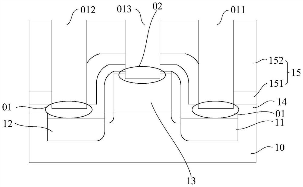
[0065] In semiconductor devices, contacts are typically formed on the gate and active regions (ie, source or drain). like figure 1 As shown, taking a CMOS device as an example, a device layer is formed in the substrate 10, and the device layer includes a source electrode 11 and a drain electrode 12 located inside the substrate and a gate electrode 13 located above the substrate. The drain has a deeper depth than the gate. An interlayer dielectric layer 15 (usually a multilayer structure, such as figure 1 When the first dielectric layer 151 and the second dielectric layer 152) and the etch stop layer 14 are etched to form the source contact hole 011, the drain contact hole 012 and the gate contact hole 013, it is usually synchronous etching, At this time if figure 1 As shown, over-etching 02 occurs at the bottom of the gate contact hole 013 with a shallow depth, and under-etching 01 occurs at the bottom of the source contact hole 011 and the drain contact hole 012 with a dee...

Embodiment 2

[0081] This embodiment also provides a method for etching a contact hole of a CMOS device. An etch stop layer containing carbon is formed above the device layer to eliminate under-etching or over-etching. The similarities between this embodiment and the contact hole etching method of the CMOS device provided in the first embodiment will not be repeated, and the differences are:

[0082] In step S102, an etch stop layer is formed over the gate electrode and the active region. When the etch stop layer is an etch stop layer containing carbon, in this embodiment, a carbon-rich layer is formed on the surface of the etch stop layer. 205 , specifically, an ion implantation method is used to implant carbon particles in the surface layer of the etch stop layer, the implantation concentration is between 1E15 cm-2 and 1E16 cm-2, and the implantation energy is less than 5Kev. The thickness of the formed carbon-rich layer 205 is also less than or equal to 1 nm.

[0083] After the carbon-r...

Embodiment 3

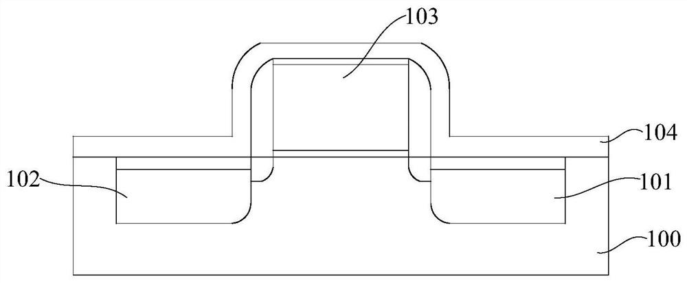
[0086] This embodiment provides a method for manufacturing a CMOS device. The method first forms a device layer on a substrate through a front-end process. Taking a CMOS device as an example, the device layer includes a gate electrode 103 , a source electrode 101 and a drain electrode 102 .

[0087] Then, using the contact hole etching method described in the first embodiment, a gate contact hole 1030 , a source contact hole 1010 and a drain contact hole 1020 are formed above the device layer. For the formation of the above-mentioned contact holes, reference may be made to the method described in the first embodiment, which will not be described in detail here. After that, as Figure 14 As shown, each contact hole is filled with conductive material to form a gate contact 130 , a source contact 110 and a drain contact 120 . In an optional embodiment, the above-mentioned conductive material to be filled is tungsten, and other conductive materials such as copper and silver may a...


PUM

PropertyMeasurementUnit
thicknessaaaaaaaaaa

Abstract

The invention provides a contact hole etching method of a CMOS (Complementary Metal Oxide Semiconductor) device and a manufacturing method of the CMOS device, which are characterized in that after a device layer is formed through a front-end process, an etching stop layer is formed on a grid electrode and an active region of the device layer, a carbon cap layer is formed on the etching stop layer, or a carbon-rich layer is formed on the surface layer of the etching stop layer through ion implantation carbon in the etching stop layer, and the carbon cap layer is formed on the surface layer of the carbon-rich layer. And forming an interlayer dielectric layer on the etching stop layer. Due to the existence of the carbon cap layer or the carbon-rich layer above the etching stop layer, when the etching stop layer with relatively shallow depth is etched, a large amount of polymer is formed in the etching stop layer, and the polymer can protect the etching stop layer to be further etched. Therefore, in the subsequent etching process of the contact hole with the relatively deep depth, the contact hole with the relatively shallow depth can be effectively protected from an over-etching phenomenon until the etching of the contact hole with the relatively deep depth is completed. Therefore, the over-etching phenomenon is avoided, the deep contact hole can be fully etched, and the phenomenon of insufficient etching is avoided.

Description

technical field [0001] The invention relates to the field of semiconductor devices, in particular to a method for etching a contact hole of a CMOS device and a method for manufacturing the CMOS device. Background technique [0002] In semiconductor devices, contacts are typically formed on the gate and active regions (ie, source or drain). In CMOS devices, the contacts on the active area are usually deeper than the contacts on the gate. In other advanced technologies, such as FDSOI (fully depleted silicon-on-insulator) and 3D NAND, there are contacts with different depths of contact with the active area. [0003] In the prior art, contact holes in semiconductor devices are usually formed by simultaneous etching. At this time, for gates and active regions with different depths, there will be contact holes with a shallow depth and over-etching will occur, and contact holes with a shallow depth will be under-etched. Whether it is over-etching or under-etching, the conductivi...

Claims


Application Information

Patent Timeline
Patent Type & Authority Applications(China)
IPC IPC(8): H01L21/768H01L21/8238
CPCH01L21/823871H01L21/76829H01L21/31116H01L21/0206H01L21/31155H01L29/7833H01L29/6659H01L21/76832H01L21/76834H01L21/76825H01L21/76816H01L21/76877H01L21/76802H01L21/31133H01L21/31138H01L29/401
Inventor 季明华孟昭生张显
Owner SIEN QINGDAO INTEGRATED CIRCUITS CO LTD
Why Eureka
Try Eureka