Test structure and test method of wafer-level integrated system

An integrated system and test structure technology, applied in the direction of single semiconductor device testing, semiconductor/solid-state device components, sorting, etc., can solve the problem of not adapting to the wafer-level system test method, and achieve the effect of ensuring reliable operation

Active Publication Date: 2022-08-02
ZHEJIANG LAB
View PDF13 Cites 3 Cited by
  • Summary
  • Abstract
  • Description
  • Claims
  • Application Information

AI Technical Summary

Problems solved by technology

[0004] At present, system-level testing is at the package level, requiring customization of specific sockets (Socket) and test boards (Loadboard), and there is currently no suitable wafer-level system testing method for SoW, a new technology of wafer-level integration.

Method used


Image

  • Test structure and test method of wafer-level integrated system
  • Test structure and test method of wafer-level integrated system
  • Test structure and test method of wafer-level integrated system

Examples


Embodiment Construction

[0033] In order to make the objectives, technical solutions and technical effects of the present invention clearer, the present invention will be further described in detail below with reference to the accompanying drawings and embodiments of the description.

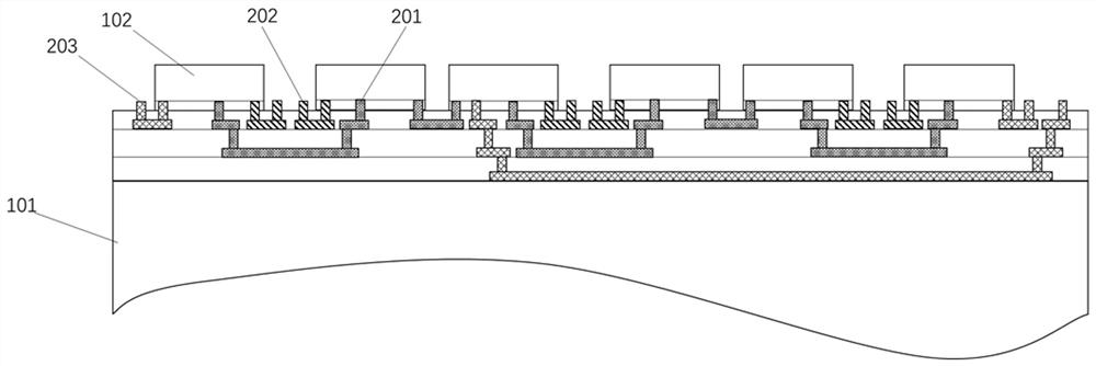
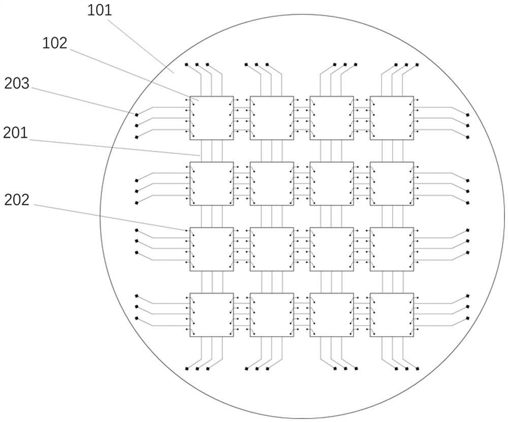
[0034] A test structure for a wafer-level integrated system, such as figure 1 and figure 2 As shown, it includes a wafer substrate 101 and n (n≥2) chips 102 bonded to the wafer, and the chips are connected to each other through the wafer electrical interconnection structure 201. The die test circuit 202 is led out from the periphery and the system test circuit 203 is led out through the inter-wafer interconnection.

[0035] The n chips form at least one complete operable system through the wafer electrical interconnection structure 201 .

[0036] The n core particles are homogeneous core particles or heterogeneous core particles.

[0037] The n core particles are all good-quality core particles sliced ​​after passin...


PUM


Abstract

The invention discloses a test structure and a test method of a wafer-level integrated system. The test structure is composed of a wafer substrate, core particles bonded on a wafer, a core particle test circuit led out from the periphery of the core particles on the wafer, and a system test circuit led out to the periphery of the wafer through wafer interconnection. According to the testing method, testing of the integrated core particles and testing of the integrated system are achieved through one-time needle inserting. The method comprises the following steps: firstly, carrying out corresponding wafer-level chip testing on homogeneous core particles, after testing the failed core particles, entering a next type of homogeneous core particle testing, and after testing all the core particles, constructing a system link according to the tested core particles, and carrying out system-level testing on a wafer-level integrated system. According to the invention, the test of the bonded core particles and the test of the on-chip integrated system can be completed through one-time needle insertion, the invalid core particles can be screened out through the core particle test, and the system-level test can ensure the correctness of a system link and the reliable operation of the whole on-chip system.

Description

technical field [0001] The invention relates to the technical field of semiconductors, and in particular, to a test structure and a test method of a wafer-level integrated system. Background technique [0002] As the integrated circuit industry enters the post-Moore's Law era, advanced integrated packaging technology has gradually become the cusp of the trend. The most representative ones are the 2.5D packaging technologies EMIB and CoWoS released by Intel and TSMC respectively. The packaging type of integrated circuits is also gradually developing from 2D packaging to 2.5D and 3D packaging, and various SoC (System on Chip) and SiP (System in package) have emerged in the field. In 2021, TSMC will further lay out the system on the wafer and release the InFO_SoW (Integrated Fan Out_System on Wafer) on-chip system technology for artificial intelligence. [0003] The realization of SoW usually relies on the bonding technology of W2W (Wafer to Wafer) or D2W (Die to Wafer) to re...

Claims


Application Information

Patent Timeline
Patent Type & Authority Applications(China)
IPC IPC(8): H01L23/544B07C5/344G01R31/26
CPCH01L22/34H01L22/32B07C5/344G01R31/2601
Inventor 王伟豪李顺斌刘冠东张汝云
Owner ZHEJIANG LAB
Why Eureka
Try Eureka