Supercharge Your Innovation With Domain-Expert AI Agents!

Cover plate and wafer etching clamp system

A fixture system and cover plate technology, which is applied in the manufacture of electrical components, circuits, semiconductors/solid-state devices, etc., can solve the problems of short service life of fixtures, wafer edge distortion, high cost, etc., achieve symmetry and improve the flatness of C surface, Avoid Distortion Effects

Pending Publication Date: 2022-08-05
广东中图半导体科技股份有限公司
View PDF0 Cites 0 Cited by
  • Summary
  • Abstract
  • Description
  • Claims
  • Application Information

AI Technical Summary

Problems solved by technology

The existing fixture system still has problems such as obvious distortion of the edge of the wafer, short service life of the fixture, and high cost during use.

Method used


Image

  • Cover plate and wafer etching clamp system
  • Cover plate and wafer etching clamp system
  • Cover plate and wafer etching clamp system

Examples


Embodiment Construction

[0020] The present invention will be further described in detail below in conjunction with the accompanying drawings and embodiments. It should be understood that the specific embodiments described herein are only used to explain the present invention, but not to limit the present invention. In addition, it should be noted that, for the convenience of description, the drawings only show some but not all structures related to the present invention.

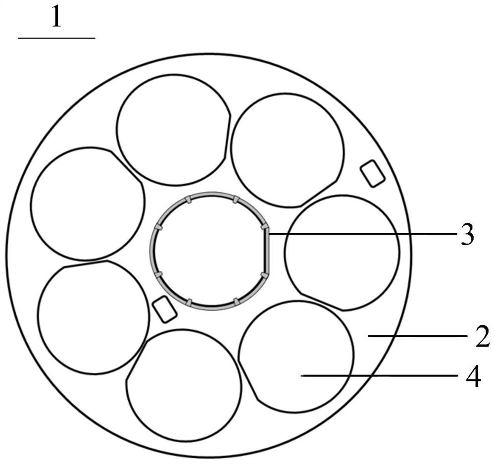
[0021] Based on the above defects of the prior art, the present invention provides a cover plate, which is applied to a wafer etching fixture system to improve the wafer edge distortion phenomenon and increase the service life of the cover plate. figure 1 A top view of a cover plate provided by an embodiment of the present invention, such as figure 1 As shown, the cover plate 1 includes a metal frame 2 and a claw structure 3; the metal frame 2 includes a plurality of openings 4, the shape of the openings 4 is the same as that of t...


PUM

PropertyMeasurementUnit
lengthaaaaaaaaaa

Abstract

The embodiment of the invention discloses a cover plate and a wafer etching clamp system. Wherein the cover plate comprises a metal frame and a pressing claw structure; the metal frame comprises a plurality of open holes, the shape of the open holes is the same as that of the wafer, and the size of the open holes is larger than that of the wafer; the pressing claw structure is installed on the edge of the opening and used for fixing the wafer. Wherein the pressing claw structure and the metal frame are made of different materials, and the difference value between the dielectric constant of the pressing claw structure and the dielectric constant of the wafer is smaller than a preset dielectric constant difference value. Through the scheme, the dielectric constant of the press claw structure is close to or the same as that of the wafer, the potentials of the contact areas of the wafer edge and the press claw structure in the etching process are basically the same, no obvious potential difference is generated, and the distortion of the wafer edge pattern caused by the angle deviation of an electric field is avoided; and the symmetry of the pattern on the etched patterned substrate and the flatness of the C surface are obviously improved.

Description

technical field [0001] Embodiments of the present invention relate to the technical field of semiconductor processing, and in particular, to a cover plate and a wafer etching fixture system. Background technique [0002] The manufacture of patterned sapphire substrate (PSS) consists of two pattern transfers. The yellow light process forms a heterogeneous glue column on the surface of the sapphire flat wafer, and the etching process uses the heterogeneous glue column as a mask to remove the excess sapphire and form Homogeneous graphics. In the etching process, in order to take into account both the efficiency and the process, a fixture composed of a tray, a cover plate, a sealing ring and a screw is generally used, and a plurality of sapphire wafers covered with heterogeneous glue columns are loaded in the middle and sent to the etching process chamber for processing. Operation. [0003] In the large-scale manufacturing process of PSS, the following requirements are placed ...

Claims


Application Information

Patent Timeline
Patent Type & Authority Applications(China)
IPC IPC(8): H01L21/687H01L21/67
CPCH01L21/68785H01L21/68771H01L21/68721H01L21/68757H01L21/68728H01L21/67109H01L21/67063
Inventor 张剑桥康凯谢鹏程吴伟陈情景陈术文陆前军
Owner 广东中图半导体科技股份有限公司
Features
  • R&D
  • Intellectual Property
  • Life Sciences
  • Materials
  • Tech Scout
  • Unparalleled Data Quality
  • Higher Quality Content
  • 60% Fewer Hallucinations
Learn More