Ceramic shell flip chip packaging laminated structure and assembling method
A ceramic shell and flip-chip technology, which is applied in the direction of semiconductor/solid-state device components, semiconductor devices, electrical components, etc., can solve the problem of inability to realize multiple flip-chip stacked structures, flip-chip interconnection obstacles, and reduce the cost of chips. To improve the effect of interconnection, broaden the scope of use, and ensure the effect of stacked connections
- Summary
- Abstract
- Description
- Claims
- Application Information
AI Technical Summary
Problems solved by technology
Method used
Image
Examples
Embodiment 1
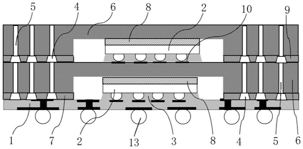
[0053] like figure 1As shown, a ceramic shell 6 flip-chip 2 package stack structure of the present invention includes a substrate 1 and at least two ceramic shells 6, wherein the substrate 1 is disposed at the bottom of the ceramic shell flip-chip package stack structure of the present invention The upper surface of the base plate 1 is respectively provided with two ceramic shells 6, the ceramic shell 6 is a rectangular structure, wherein the center of one end face of the rectangular structure is provided with a through groove penetrating the horizontal direction, and the two ceramic shells 6 include a first ceramic shell. and the second ceramic shell, the structure and shape of the first ceramic shell and the second ceramic shell are the same, wherein, the first ceramic shell is arranged on the substrate 1 and is fixedly connected with the substrate 1, and the second ceramic shell is arranged on the first ceramic shell. The upper surface of the ceramic shell is fixedly connec...
Embodiment 2
[0066] A method for assembling a ceramic shell flip-chip package stack structure, such as Figure 15 shown, including:
[0067] S1: set metal circuit connection points on the upper and lower surfaces of the substrate 1;
[0068] S2: The insulating layer body on the substrate 1 is arranged on the left and right sides of the upper surface of the substrate 1, and the metal bump 4 and the columnar metal 5 are arranged on the set insulating layer body;
[0069] S3: solder the solder balls 13 on the bottom surface of the flip chip 2 to the metal pads 10 on the upper surface of the substrate 1, and fill the protective colloid 3 between the lower surface of the chip and the upper surface of the substrate 1;
[0070] S4: set the first ceramic shell 6 above the insulating layer body on the set substrate 1;
[0071] S5: set metal pads 10 on the first ceramic shell 6, set the ceramic shell upper insulating layer 9, bump chips and metal bumps 4 on the set metal pads 10, set on the metal ...
PUM
 Abstract
Description
Claims
Application Information


