Method for forming copper layer on semiconductor chip

A chip and copper layer technology, applied in the direction of semiconductor devices, semiconductor/solid-state device manufacturing, semiconductor/solid-state device components, etc., can solve problems such as expensive, unreliable, time-consuming, etc., to optimize productivity, reduce utilization rate, improve performance effect

Inactive Publication Date: 2005-04-13
VLSI TECH LLC
View PDF0 Cites 2 Cited by
  • Summary
  • Abstract
  • Description
  • Claims
  • Application Information

AI Technical Summary

Problems solved by technology

[0008] The overall method of processing the test wafers, determining the static conditions under which the test wafers give good results, and using these conditions to statically process the wafers with continued hope of success is time consuming, unreliable, and expensive

Method used


Image

  • Method for forming copper layer on semiconductor chip
  • Method for forming copper layer on semiconductor chip
  • Method for forming copper layer on semiconductor chip

Examples


Embodiment Construction

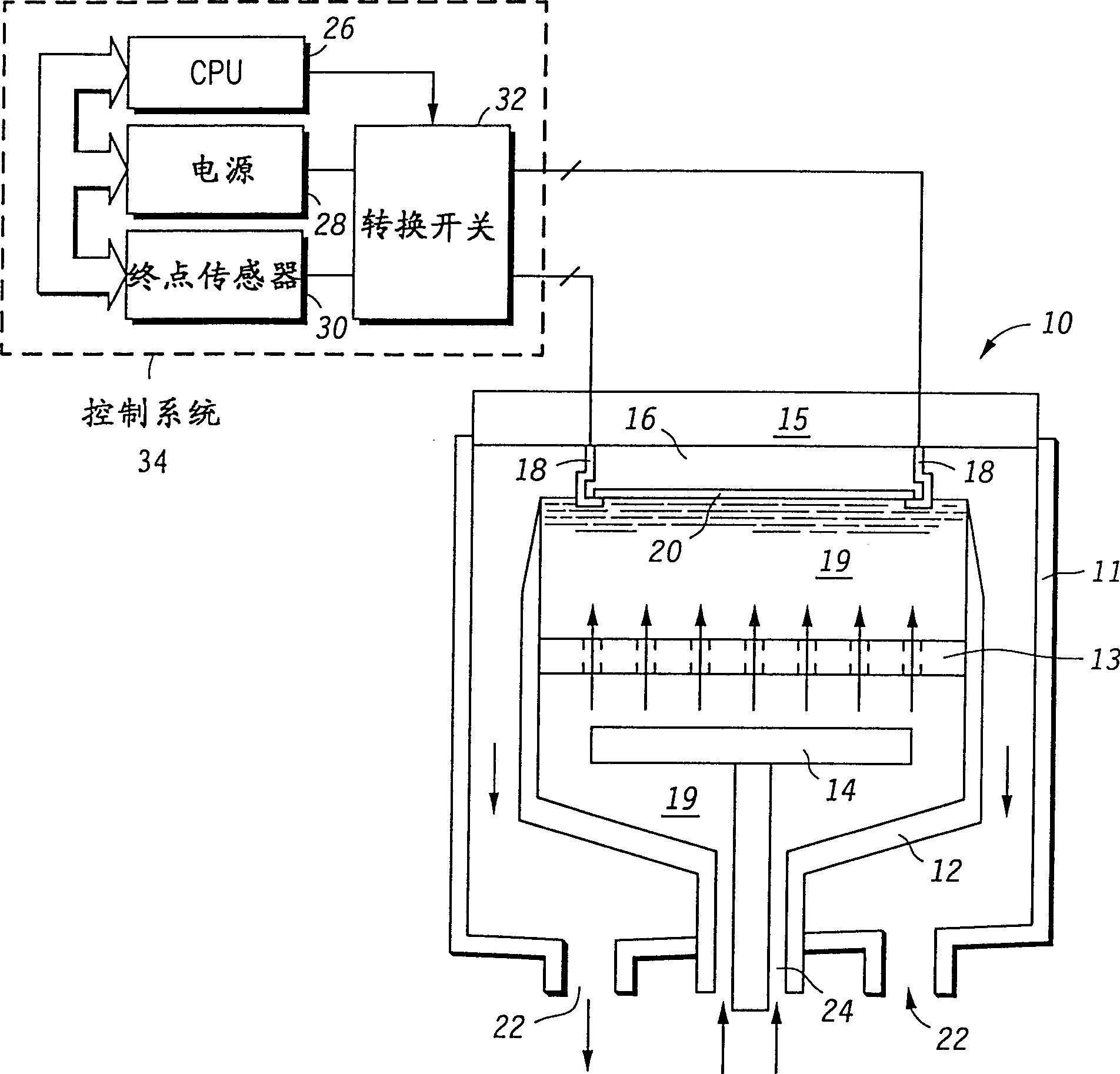
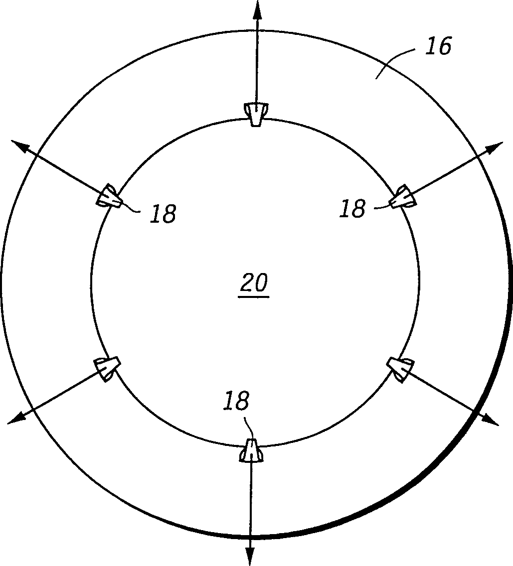
[0021] In general, the present invention is a method and apparatus for controlling the cathode and / or anode of a copper electroplating chamber to improve the quality of copper (Cu or Cu alloy) interconnects formed on semiconductor wafers through copper electroplating operations. It has been found that various pulsed positive and / or negative current waveform sequences with various optional direct current (DC) bias cycle inclusions can have significant effects on copper uniformity, copper resistance to electromigration (EM), plating productivity, One or more of copper voiding, copper grain structure, and / or similar properties can adversely affect the aforementioned various optional DC bias cycles applied to the cathode and / or anode of the copper electroplating chamber.

[0022] The improved copper electroplating method taught herein is by specific reference to Figure 1-13 can be better understood.

[0023] figure 1 A cross-sectional view of an electroplating system or chamber...


PUM


Abstract

A method for electroplating a copper layer (118) over a wafer (20) powers a cathode of an electroplating system (10) in a manner that obtains improved copper interconnects. A control system (34) powers the cathode of the system (10) with a mix of two or more of: (i) positive low-powered DC cycles (201 or 254); (ii) positive high-powered DC cycles (256 or 310); (iii) low-powered, pulsed, positive-power cycles (306 or 530); (iv) high-powered, pulsed, positive-powered cycles (212, 252, 302, or 352); and / or (v) negative pulsed cycles (214, 304, 510, 528, or 532). The collection of these cycles functions to electroplate copper or a like metal (118) onto the wafer (20). During electroplating, insitu process control and / or endpointing (506, 512, or 520) is performed to further improve the resulting copper interconnect. <IMAGE>

Description

technical field [0001] The present invention relates generally to semiconductor manufacturing techniques, and more particularly to a method of electroplating copper on a semiconductor substrate to form damascene copper interconnects. Background technique [0002] Current semiconductor devices require higher current densities for better performance. Furthermore, the size of devices is shrinking to geometries, which becomes increasingly problematic when conducting higher current densities. Existing technologies must be used to accommodate higher current densities while simultaneously maintaining sufficient resistance levels for electromigration (EM), reduced metal voids, improved wafer production throughput, and also avoiding other common reliability issues and reduced geometry. While aluminum is a well-established interconnect material for integrated circuits (ICs), copper is a relatively new material for IC interconnects. [0003] One of the most promising methods for dep...

Claims


Application Information

Patent Timeline
IPC IPC(8): H01L21/283H01L21/3205H01L21/768C25D5/18C25D7/12H01L21/28H01L21/288H01L23/52
CPCH01L21/2885H01L21/76877H01L21/28
Inventor 辛迪·雷德西马·辛普森罗伯特·道格拉斯·米考拉马修·T·赫里克布勒特·卡罗琳·贝克尔戴维·摩拉勒兹·皮那爱德华·阿考斯塔利那·超德胡瑞马利金·阿兹拉克辛迪·凯·高尔德博格默罕穆德·拉比优尔·伊斯拉姆
Owner VLSI TECH LLC
Why Eureka
Try Eureka