
System and method for reducing welding program error for IC welding machine

A welding procedure, integrated circuit technology, applied in the direction of circuit, program control, welding equipment, etc., can solve the problem of time-consuming and so on

Inactive Publication Date: 2005-07-20
TEXAS INSTR INC
View PDF4 Cites 0 Cited by
  • Summary
  • Abstract
  • Description
  • Claims
  • Application Information

AI Technical Summary

Problems solved by technology

The regeneration process has many steps, so there are many opportunities for human error
[0019] * Time-consuming to perform alignment regeneration: Operators have to spend a lot of time doing alignment regeneration whenever a device is to be soldered

Method used


Image

  • System and method for reducing welding program error for IC welding machine
  • System and method for reducing welding program error for IC welding machine
  • System and method for reducing welding program error for IC welding machine

Examples


Embodiment Construction

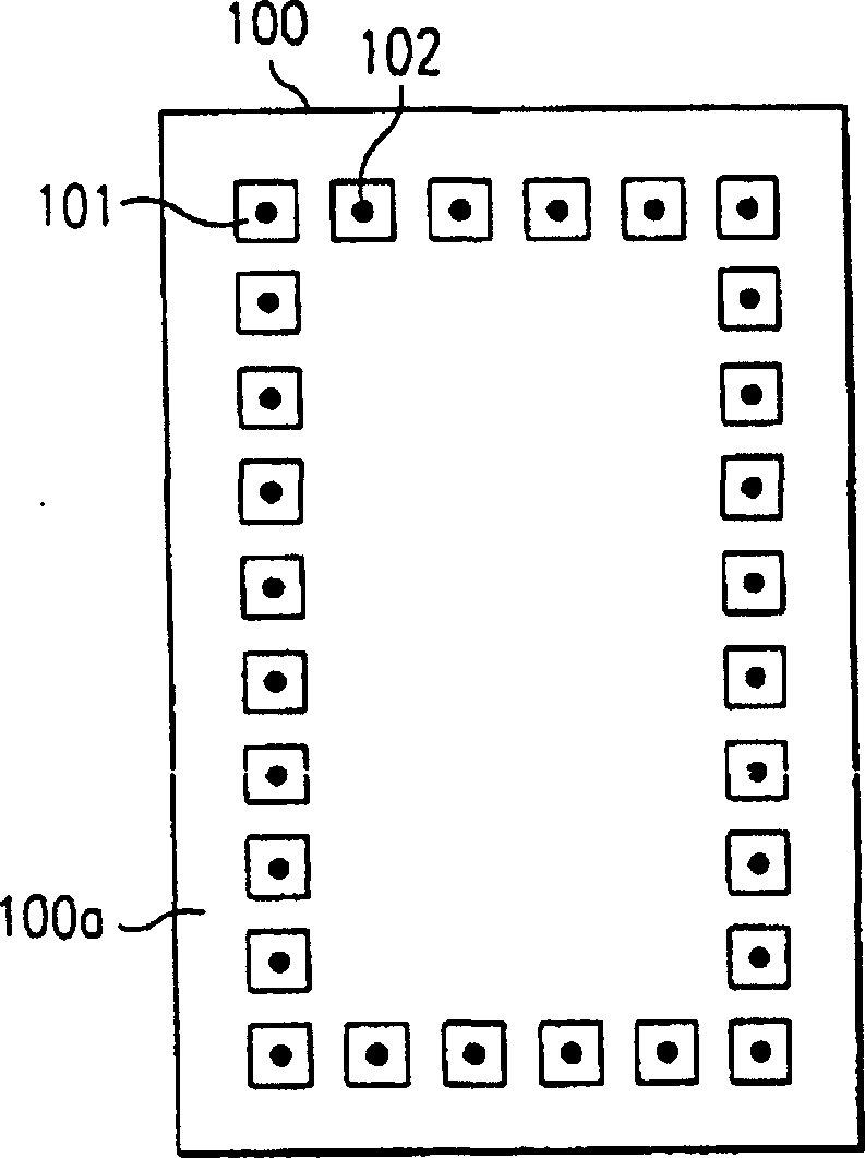
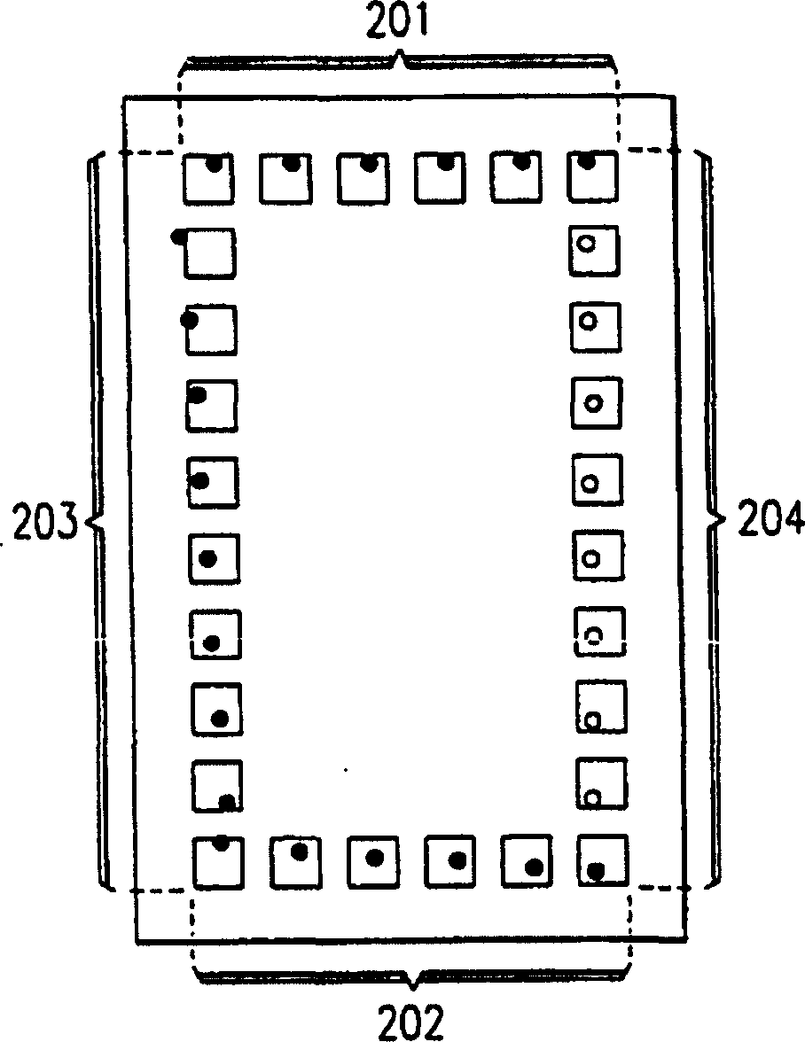
[0042] figure 1 and 2 Examples illustrate the problems and errors that the present invention solves in semiconductor chip assembly and bonding operations. figure 1 In this example, a plurality of bonding pads 101 are placed on the active surface 100 a of the chip 100 . In the ideal assembly situation shown, all of the adhesive 102 attached to the pad 101 is located in the center of the pad area. figure 2 , similar pads are shown, but the adhesive deviates from the ideal position in several ways. In the top row of pads 201, all adhesive is biased towards the perimeter of the pads (here representing a risk to the quality of the soldering and the reliability of the material surrounding the pad area). In the bottom row 202 of pads, the adhesive gradually slopes (some of which will be outside the range of acceptable soldering). In the left column 203 of pads, the adhesive also slopes gradually (so that some of the adhesive comes off the pads). In the right column of pads 204,...


PUM


Abstract

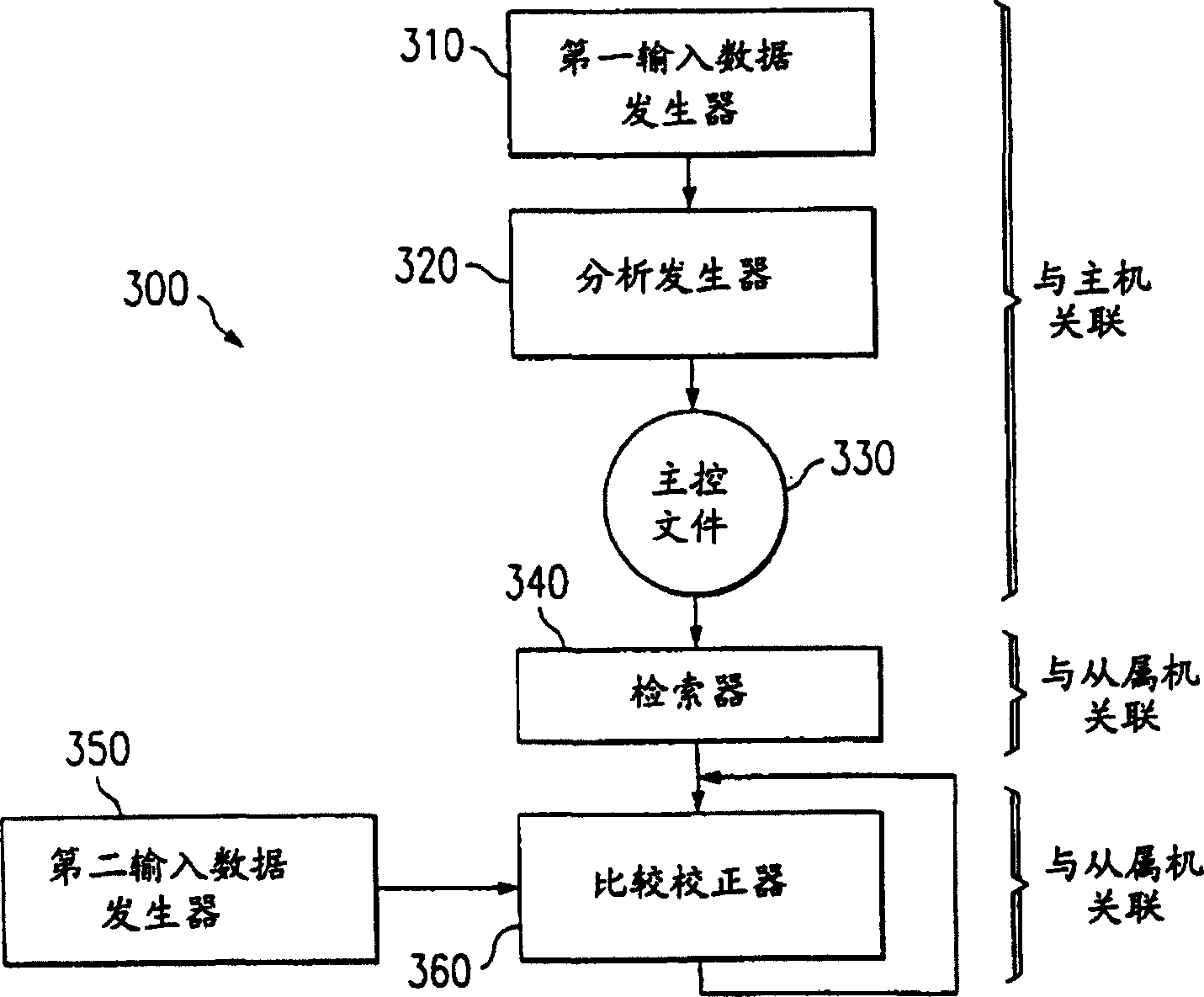
A computerized system and method for reducing bond program errors in a slave bonder, prepared to attach connecting bonds onto bond pads of a slave integrated circuit, by first collecting, on a master bonder, input data concerning bond x-y locations, alignment reference x-y locations, and alignment reference images from a master integrated circuit, then analyzing these data to construct a network of relationships between reference images and bond locations, and store data and relationships in a master file. Secondly, on a slave bonder, all this information is automatically retrieved and compared by a computer with input data concerning alignment reference images from a slave circuit. Thirdly, any discrepancy found is corrected by a computer to identify the new bond locations on the slave circuit. Finally, the slave bonder attaches the connecting bonds based on the computed correct bond locations.

Description

technical field [0001] The present invention generally relates to the field of semiconductor devices and electronic systems, and more particularly to an error-reducing device and operating method for computer-controlled welding machines for integrated circuit assemblies. Background technique [0002] In an integrated circuit (IC) package, the IC chip is typically mounted on a lead frame and electrically connected to it by metal segments. Chip components are generally encapsulated in a protective package (such as a ceramic package or a plastic package using a molding process). Typically, an IC chip has a plurality of pads positioned generally around the perimeter of the chip with a predetermined bonding area and spacing (pad pitch). The wireframe typically has narrow "inner" leads that connect to segments and contents within the package, and wide "outer" leads that connect to other parts such as solder to the circuit board. [0003] The metal segments used to electrically c...

Claims


Application Information

Patent Timeline
Patent Type & Authority Patents(China)
IPC IPC(8): H01L21/60B23K1/00G05B19/4093G06F9/00H01L21/50H01L23/488
CPCG05B2219/49113G05B19/4093G05B2219/45029G05B2219/45026G05B2219/45235H01L24/78H01L24/85H01L2224/78H01L2224/85H01L2924/00014H01L2924/14H01L2224/05554H01L2224/45014Y02P90/02H01L2224/45099H01L2224/05599H01L2924/00H01L2924/206H01L21/60
Inventor S·K·科杜里D·J·博恩
Owner TEXAS INSTR INC
Learn More