Detection method of dynamic micronic dust in etching reaction chamber

A technology of pollution state and detection method, which is applied in the direction of optical testing of flaws/defects, discharge tubes, electrical components, etc., can solve the problems of not being able to react in real time to the etching reaction chamber, affecting the process performance and product pass rate, etc., to increase production capacity and reduce costs Effect

Inactive Publication Date: 2005-08-03
MACRONIX INT CO LTD
View PDF0 Cites 2 Cited by
  • Summary
  • Abstract
  • Description
  • Claims
  • Application Information

AI Technical Summary

Problems solved by technology

However, it takes at least half a day before the product is in the etching reaction chamber to carry out the etching process when it is detected that there is a problem with the product, and it takes half a day to inspect the dust after the shutdown. Therefore, the known method cannot respond in real time. The condition of the etching reaction chamber, and it is easy to affect the performance of the process and the pass rate of the product

Method used


Image

  • Detection method of dynamic micronic dust in etching reaction chamber
  • Detection method of dynamic micronic dust in etching reaction chamber
  • Detection method of dynamic micronic dust in etching reaction chamber

Examples


Embodiment Construction

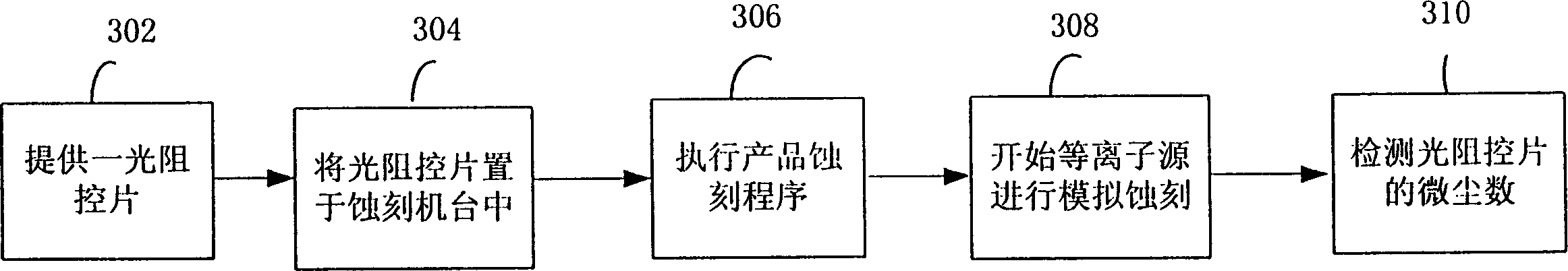
[0022] The invention uses the photoresist control sheet to simulate the conveying process of the actual production of the product in the etching process, and actually executes the production etching program, which can effectively simulate the situation that the product is polluted by fine dust in the etching reaction chamber during the actual production .

[0023] The following is to disclose preferred embodiments of the present invention, and please refer to the accompanying drawings for a detailed description. Before carrying out the method for detecting the dynamic fine dust pollution state of the etching reaction chamber disclosed in the present invention, the product is placed in a defect inspection machine to check the amount of fine dust. If the amount of fine particles on the product exceeds a certain value, there will be problems with the product. And the product is placed in a scanning electron microscope (Scanning Electron Microscope, SEM) to check the state of the ...


PUM


Abstract

A detecting method for the state of micro-dust pollution features that a photoresistive control piece put on the etching machine is transported to the main etch room. With the plasma source being started, the procedure for etching the photoresistive layer of the control piece is carried out. Then, the number of microparticles on the control piece etched is determined, in order to judge the state of the etching machine.

Description

technical field [0001] The invention relates to a method for detecting the state of an etching machine, and in particular to a method for detecting the state of dynamic fine dust pollution in an etching reaction chamber. Background technique [0002] The etching process can be said to be one of the most important steps in the entire semiconductor process. Generally speaking, the device pattern on the photomask is firstly transferred to the photoresist by a lithography process. Then, the etching process is used to complete the final purpose of transferring the entire pattern to the film. This lithographic and etched film will become part of the semiconductor device. Taking the manufacturing process of MOS or CMOS as an example, this layer of film may be silicon dioxide (SiO 2 ), silicon nitride (Si 3 N 4 ), polycrystalline silicon (Poly-Si), aluminum alloy (Al Alloy) or phosphosilicate glass (Phosphosilicate, PSG), etc. That is to say, almost the main materials of semic...

Claims


Application Information

Patent Timeline
Patent Type & Authority Patents(China)
IPC IPC(8): G01N21/89G01N21/94H01J37/28
Inventor 林明裕陈威铭黄彦智林世丰
Owner MACRONIX INT CO LTD
Why Eureka
Try Eureka