Semiconductor memory and semiconductor memory control method
A semiconductor and memory technology, applied in the field of semiconductor memory, can solve the problems that the average current consumption cannot be effectively reduced, and the current consumption of peripheral circuits cannot be reduced by the leakage current flowing through the word line.
- Summary
- Abstract
- Description
- Claims
- Application Information
AI Technical Summary
Problems solved by technology
Method used
Image


Examples
no. 1 example
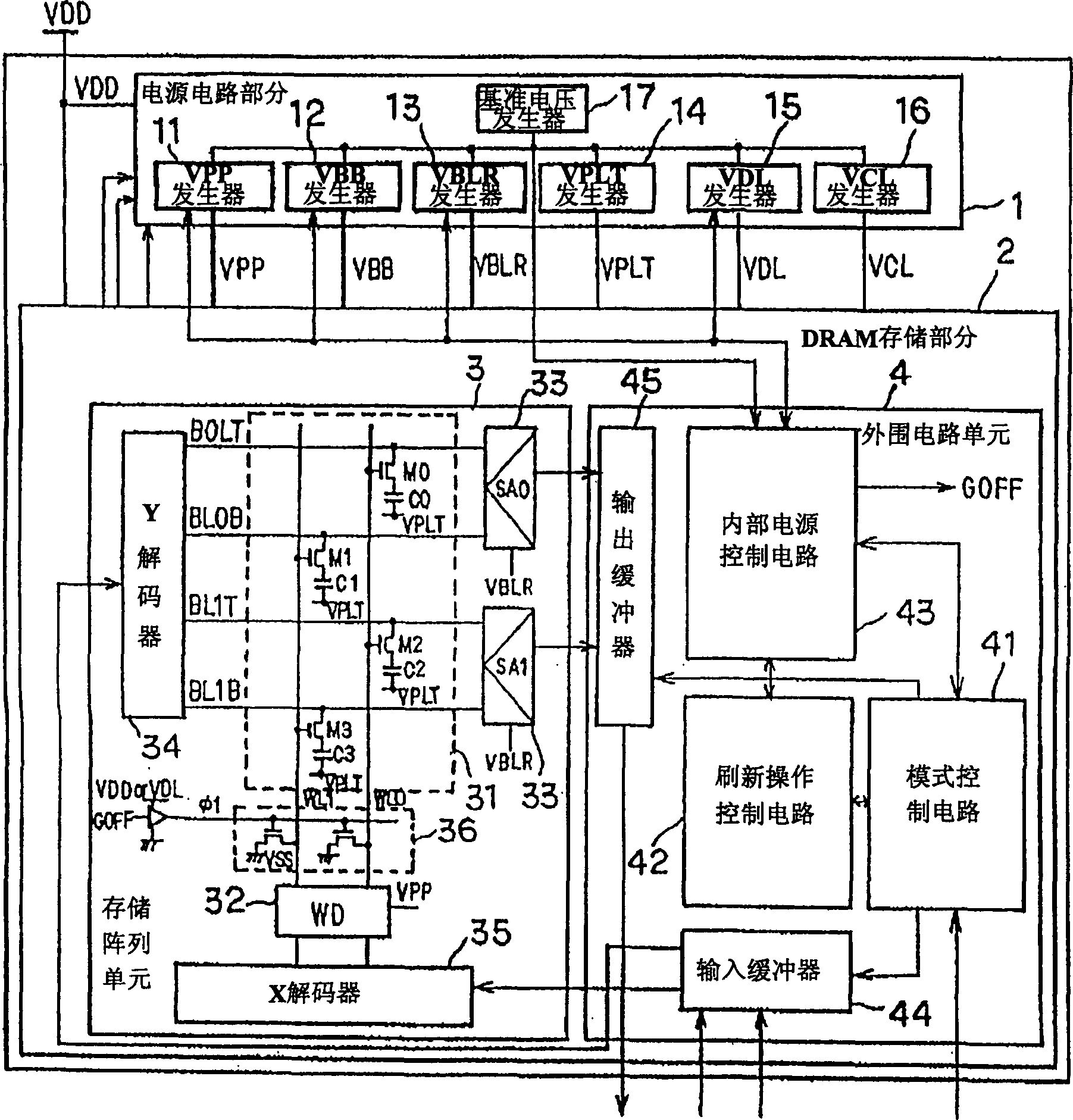
[0035] figure 1 The configuration of the semiconductor memory according to the first embodiment of the present invention is shown. Specifically, figure 1 A typical configuration of a DRAM is shown.
[0036] Such as figure 1 As shown, the semiconductor memory according to the first embodiment includes: a power supply circuit section 1 including internal voltage generator circuits respectively for generating predetermined internal power supply voltages; and a DRAM storage section 2 including a memory array unit for holding data and control circuits.
[0037] The power supply circuit part 1 includes: VPP internal voltage generator circuit 11 (VPPGENE.), used to generate word line voltage VPP; VBB internal voltage generator circuit 12 (VBBGENE.), used to generate memory array substrate voltage VBB; VBLR internal The voltage generator circuit 13 (VBLR GENE.) is used to generate the bit line precharge voltage VBLR; the VPLT internal voltage generator circuit 14 (VPLT GENE.) is u...
no. 2 example
[0084] Figure 13 A semiconductor memory configuration according to a second embodiment of the present invention is shown.
[0085] In the second embodiment, the VPP internal voltage generator circuit 11 for generating the word line voltage VPP is not stopped according to the internal power supply stop signal GOFF output from the internal power supply control circuit 43 . Furthermore, in the second embodiment, the word line voltage is applied to the source and substrate of each pMOS in the word driver applying the word line voltage VPP and the logic circuit in the X decoder, etc., respectively, as Figure 13 shown. Furthermore, a switching transistor Q100 is provided between the output terminal of the VPP internal voltage generator circuit 11 and the source of the pMOS transistor for disconnecting them. The rest of the configuration of the semiconductor memory according to the second embodiment is similar to that of the first embodiment, and thus will not be described.
[008...
PUM
 Abstract
Description
Claims
Application Information