Unlock instant, AI-driven research and patent intelligence for your innovation.

Chip having input and output terminal configurable function and method thereof

A technology of input and output terminals and input and output ports, which is applied in the direction of electrical components, electrical solid devices, circuits, etc., can solve the problems of expensive processing costs, affecting signal transmission effects, multi-layer wiring and increasing the length of wiring, etc., to reduce PCB Effects of processing cost, reducing space occupied by wiring, and reducing design cost

Inactive Publication Date: 2006-04-19
VIMICRO CORP
View PDF0 Cites 0 Cited by
  • Summary
  • Abstract
  • Description
  • Claims
  • Application Information

AI Technical Summary

Problems solved by technology

[0004] However, the wiring process of this kind of multilayer substrate is complicated, the processing cost is expensive, and the multilayer wiring increases the length of the connection, thereby reducing the integrity of the signal and affecting the signal transmission effect. At the same time, because some packaged substrates cannot be used for wiring, Such as LPCC packaging, making MCM packaging infeasible

Method used


Image

  • Chip having input and output terminal configurable function and method thereof
  • Chip having input and output terminal configurable function and method thereof
  • Chip having input and output terminal configurable function and method thereof

Examples


Embodiment Construction

[0021] In the following description, well-known functions or structures will not be described in detail to avoid unnecessary confusion with the content of the present invention.

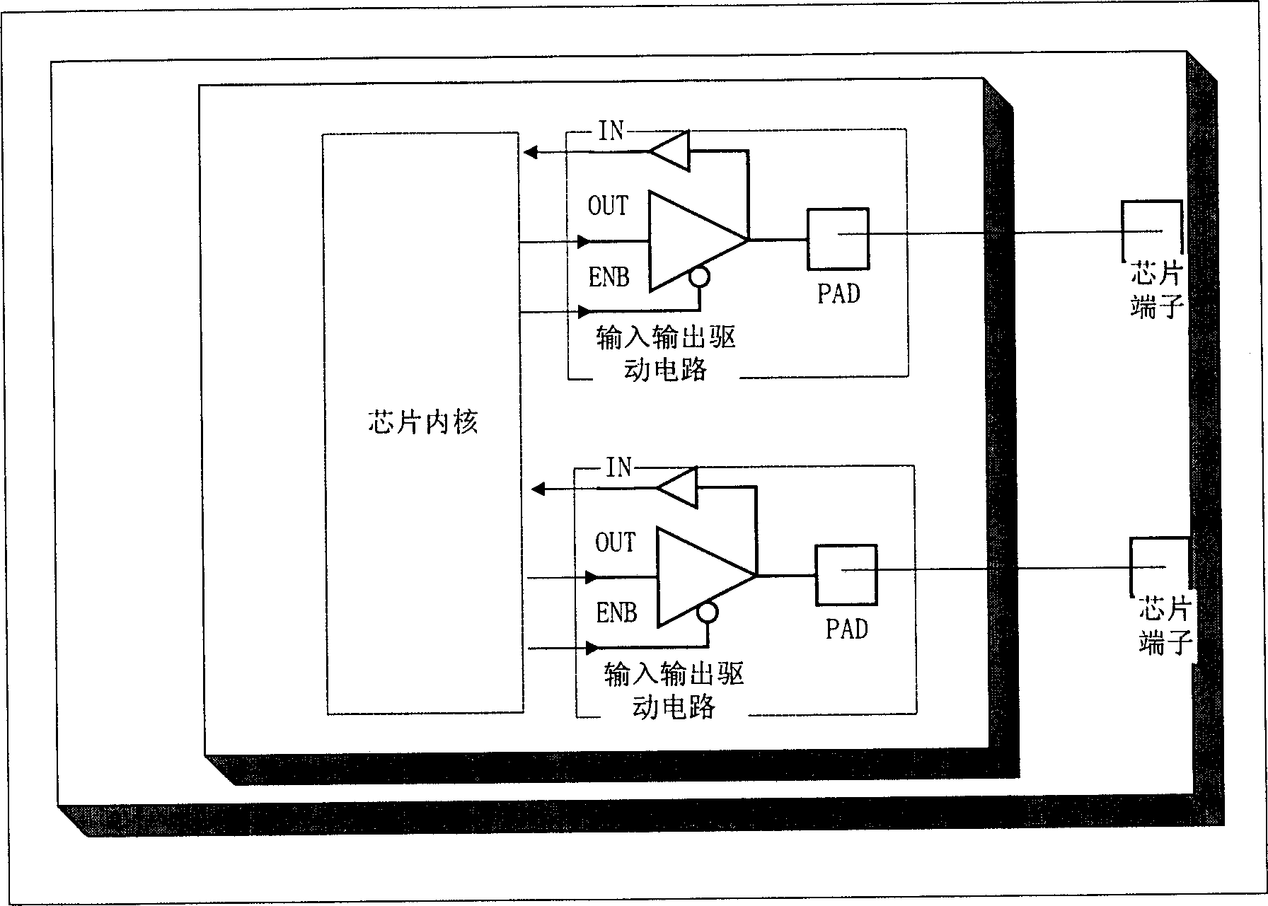
[0022] In the chip design process, an input and output drive circuit with both input and output functions is selected, and its input and output functions are controllable, such as figure 1 Shown is a common chip die structure diagram:

[0023] Input and output drive circuit (I / O BUF): it includes input terminal (IN), output terminal (OUT), output enable control terminal (ENB) and connection pad (PAD);

[0024] Chip core (CORE Logic): its input and output signals and I / O control signals are connected to the corresponding terminals of the input and output drive circuits;

[0025] Chip terminal (PIN): Since the chip pin (PIN) and the pad (PAD) on the die are usually in one-to-one correspondence after the chip is packaged, they are collectively referred to as input and output terminals for the convenien...


PUM


Abstract

The invention refers to a chip which has configuration function for input and output connector. It includes chip core part, controllable input and output driving circuit group, chip connector group; the character lies in: it also includes several mapping converting unit and a mapping control unit, the input port needing configuration function in chip core is connected to the input end of the several input and output driving circuit through a mapping converting unit, the several output port of the chip core is connected to the output end of input and output driving circuit through a mapping converting unit, and controls it. By using the invention, the chip can be connected to several chips with incompatible pins effectively, thus it decreases the volume of device greatly, upgrades the integrity of signal, reduces the complexity of components connection, and reduces the space occupied by wire, decreases the design and process cost.

Description

technical field [0001] The invention relates to the field of integrated circuit design, in particular to a chip with configurable input and output terminals and a method thereof. Background technique [0002] Modern electronic systems usually contain a large number of electronic components. People hope that the space occupied by the components and their interconnections should be as small as possible, so as to improve the portability of the equipment. This is especially urgent in mobile communications and personal handheld devices. For this reason, the MCM packaging method came into being. It encapsulates multiple chip dies in one packaging module. This method not only greatly reduces the volume of the device and reduces the space occupied by the device interconnection, but also shortens the distance between the device interconnections. The signal integrity between components is greatly improved, and the manufacturing cost is reduced by reducing the number of components in t...

Claims


Application Information

Patent Timeline
Patent Type & Authority Patents(China)
IPC IPC(8): H01L27/00H01L21/82
Inventor 金传恩张韵东
Owner VIMICRO CORP