
Method for improving anodic surface toughness of organic LED

A technology of light-emitting diodes and surface roughness, applied in electrical components, circuits, semiconductor devices, etc., can solve the problems of the surface roughness of the anode layer and the uneven thickness of the anode layer, so as to avoid the arc phenomenon and improve the surface roughness of the film layer. , the effect of reducing costs

Inactive Publication Date: 2006-05-24
AU OPTRONICS CORP
View PDF1 Cites 0 Cited by
  • Summary
  • Abstract
  • Description
  • Claims
  • Application Information

AI Technical Summary

Problems solved by technology

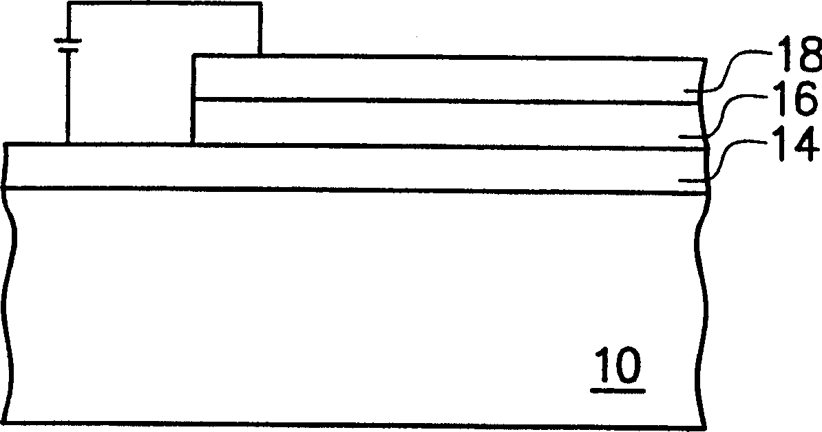
[0008] The object of the present invention is to provide a method for improving the surface roughness of the anode of an organic light-emitting diode, to solve the known problem that arcing is easy to occur when forming an anode layer with a thick film thickness, which causes the surface of the anode layer to be relatively rough and makes the anode The problem of uneven film thickness of the layer

Method used

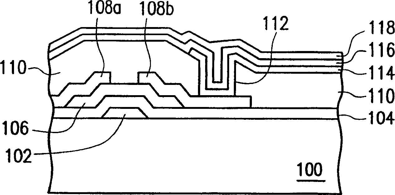

Image

  • Method for improving anodic surface toughness of organic LED
  • Method for improving anodic surface toughness of organic LED
  • Method for improving anodic surface toughness of organic LED

Examples


Embodiment Construction

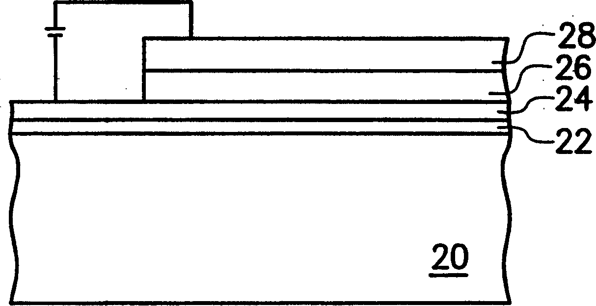
[0029] figure 2 , which is a schematic cross-sectional view of an organic light emitting diode device according to a preferred embodiment of the present invention.

[0030] Please refer to figure 2 , the manufacturing method of the organic light emitting diode device of the present invention first provides a substrate 20, wherein the substrate 20 is, for example, a glass substrate or a transparent plastic substrate. Next, a first anode layer 22 is formed on the substrate 20 , and then a second anode layer 24 is formed on the first anode layer 22 . The first anode layer 22 and the second anode layer 24 together serve as the anode electrode film of the OLED device.

[0031] Wherein, the method for forming the first anode layer 22 and the second anode layer 24 is, for example, the sputtering method, and in this embodiment, the power value of the first anode layer 22 and the second anode layer 24 formed by the sputtering method can be between Between 230W and 680W, preferably...


PUM


Abstract

A method for improving the surface roughness of an anode of an organic light-emitting diode. The method firstly provides a substrate. Next, at least two anode layers are formed on the substrate by multiple sputtering steps. Then a light emitting layer is formed on the surface of the anode layer, and a cathode layer is formed on the light emitting layer.

Description

technical field [0001] The present invention relates to a method for manufacturing an organic light emitting diode, and in particular to a method for improving the surface roughness of an anode of the organic light emitting diode. Background technique [0002] Organic light-emitting diodes are semiconductor devices that can convert electrical energy into light energy and have high conversion efficiency. Common applications are light-emitting devices for indicator lights, display panels, and optical read-write heads, etc. Due to the characteristics of organic light-emitting diode devices, such as no viewing angle, simple manufacturing process, low cost, high response speed, wide operating temperature range and full color, etc., which meet the requirements of display characteristics in the multimedia era, it has become a research boom in recent years. [0003] The basic structure of an organic light emitting diode includes a glass substrate, a metal electrode, an indium tin ox...

Claims


Application Information

Patent Timeline
Patent Type & Authority Patents(China)
IPC IPC(8): H01L33/00
Inventor 李信宏苏志鸿陈宗辉
Owner AU OPTRONICS CORP
Learn More