Repeatedly usable unpatterned wafer and forming method thereof

A technology of wafer and amorphous silicon layer, which is applied in the field of wafer control and can solve the problems of low cost of wafer control and the like

Inactive Publication Date: 2006-08-16
SEMICON MFG INT (SHANGHAI) CORP +1
View PDF0 Cites 3 Cited by
  • Summary
  • Abstract
  • Description
  • Claims
  • Application Information

AI Technical Summary

Problems solved by technology

[0004] However, the cost of the traditional wafer control wafer is not low for the semiconductor manufacturing process because the process maker of the traditional wafer control wafer can only be used once.

Method used


Image

  • Repeatedly usable unpatterned wafer and forming method thereof
  • Repeatedly usable unpatterned wafer and forming method thereof
  • Repeatedly usable unpatterned wafer and forming method thereof

Examples


Embodiment Construction

[0012] The direction of the present invention discussed here is a method for forming a wafer controller for semiconductor manufacturing process. In order to provide a thorough understanding of the present invention, detailed steps will be set forth in the following description. Obviously, the practice of the present invention is not limited to the specific details familiar to those skilled in semiconductor processing. In other instances, well-known elements or process steps have not been described in detail in order to avoid unnecessarily limiting the invention. The preferred embodiments of the present invention will be described in detail as follows, but in addition to these detailed descriptions, the present invention can also be widely implemented in other embodiments, and the scope of the present invention is not limited, which is subject to the scope of the patents that follow .

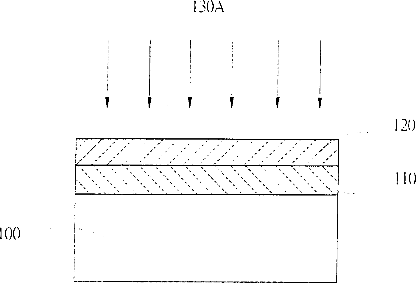
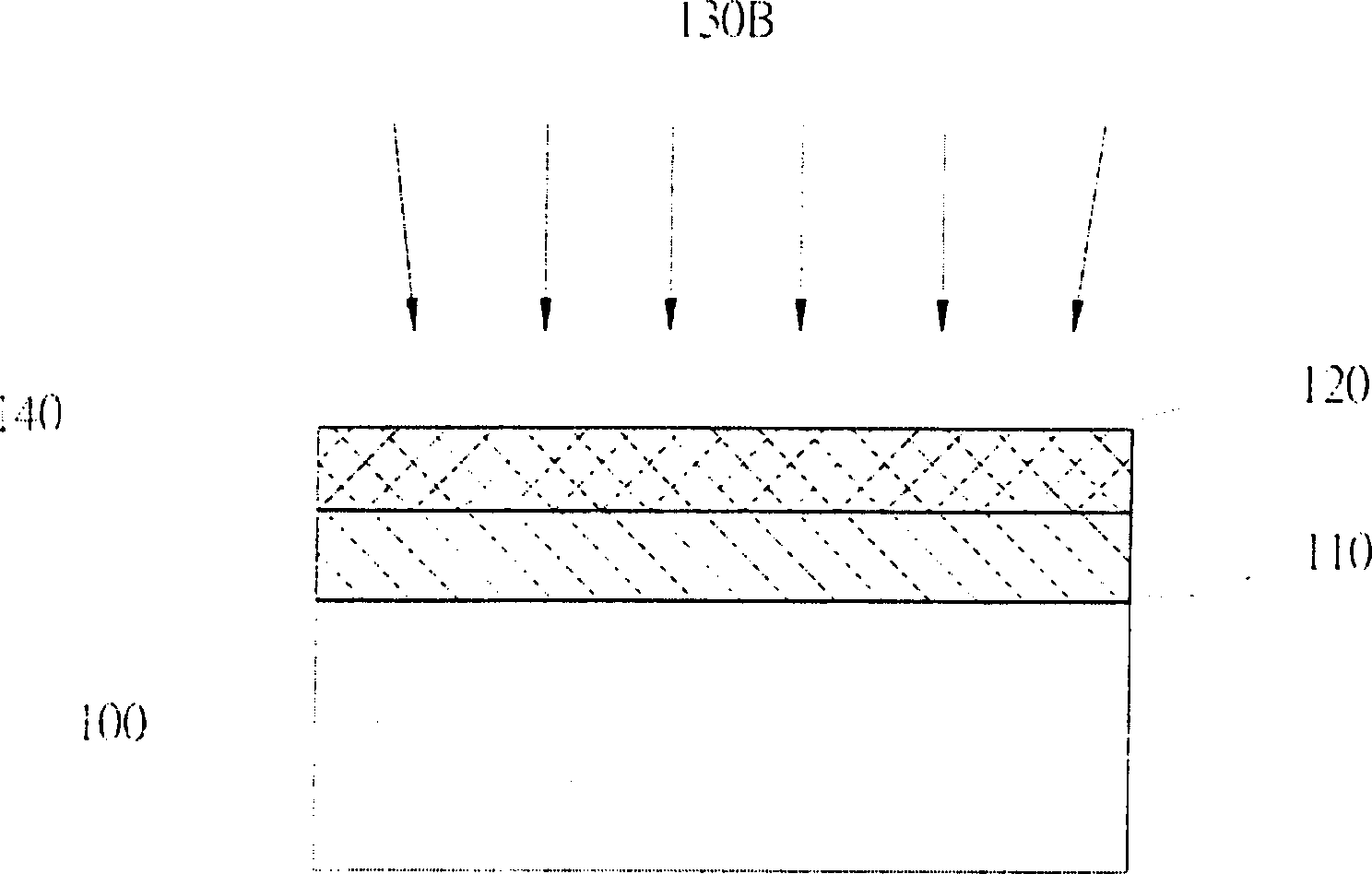
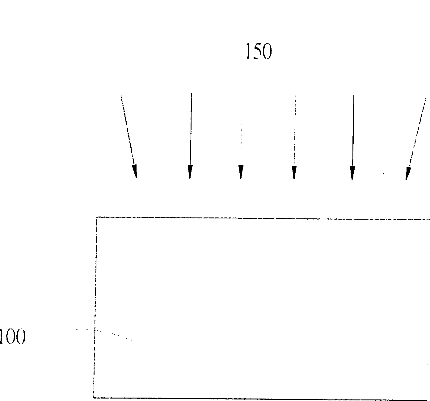
[0013] refer to Figure 1A to Figure 1C As shown, in the first embodiment of the present i...


PUM


Abstract

This invention discloses a forming method for a unpatterned water of a semiconductor process. A basic material is provided first, then an oxidation layer is formed on it and a non-crystallosilicon layer is formed, after that an ion implantation process is carried out for doping the non-crystallosilicon layer and oxidation layer. Secondly, a temper process is taken to form a unpatterned wafer and Rs is tested after that and schedule monitor is done, the non-crystallosilicon layer and oxidation layer on the moisture control plate basic material and the unpatterned wafer can be used repeatedly to reduce schedule monitor cost.

Description

technical field [0001] The invention relates to a method for forming a wafer control sheet, in particular to a method for forming a reusable wafer control sheet. Background technique [0002] As the integration of semiconductor elements continues to expand, such as Metal-Oxide-Semiconductor (MOS) elements, in order to keep the area of ​​the chip (chip) the same, or even shrink it, in order to continuously reduce the unit cost of the circuit, the only The method is to continuously reduce the circuit design rules to meet the future development trend of the high-tech industry. Therefore, the space occupied by components is also gradually reduced with the circuit design rules. With the development of semiconductor technology, the dimensions of components of integrated circuits have been reduced to the deep sub-micron range. As semiconductors continue to shrink down to the deep sub-micron range, some problems arise in process scaling. A very large scale integrated circuit (VLSI...

Claims


Application Information

Patent Timeline
Patent Type & Authority Patents(China)
IPC IPC(8): H01L21/66H01L21/00
Inventor 吴金刚黄晋德刘靓一李修远
Owner SEMICON MFG INT (SHANGHAI) CORP
Why Eureka
Try Eureka