
Semiconductor apparatus and its making method

A manufacturing method and semiconductor technology, applied in the direction of semiconductor/solid-state device manufacturing, semiconductor devices, electrical components, etc., can solve the problems of inability to achieve withstand voltage, increase and increase of short-channel effect, etc., and achieve high withstand voltage. Effect

Inactive Publication Date: 2006-10-18
SANYO ELECTRIC CO LTD
View PDF0 Cites 0 Cited by
  • Summary
  • Abstract
  • Description
  • Claims
  • Application Information

AI Technical Summary

Problems solved by technology

⑥The injected electrons reach the drain region 57, which further causes avalanche multiplication
[0015] In addition, in order to improve the operating withstand voltage (VSUS), such as Image 6 As shown in , it is also considered to increase the amount of ion implantation and increase the concentration of the N-type drain region, but as shown by the white circle in the figure, it is not possible to achieve a sufficient improvement in withstand voltage
Furthermore, conversely due to Figure 12 The concentration of the end A of the N-type drain region 56 shown in FIG. , and the increase of the snap back (rapid return) phenomenon caused by the increase of the peak value of the substrate current (I Sub), and furthermore, the drop of the voltage between the source and the drain (BVDS), so far, has not yet sought the operating withstand voltage effective way to improve

Method used


Image

  • Semiconductor apparatus and its making method
  • Semiconductor apparatus and its making method
  • Semiconductor apparatus and its making method

Examples


Embodiment Construction

[0042] Hereinafter, embodiments of the semiconductor device and its manufacturing method according to the present invention will be described with reference to the drawings.

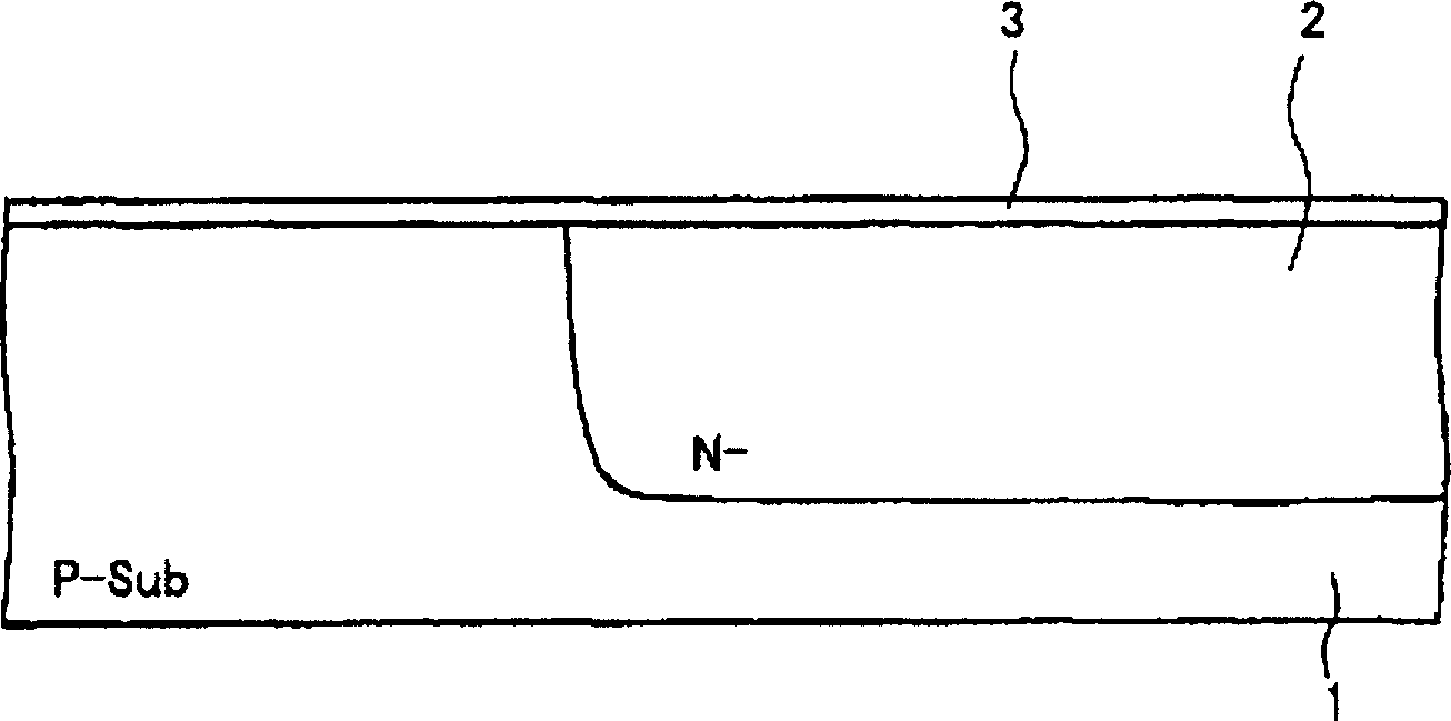
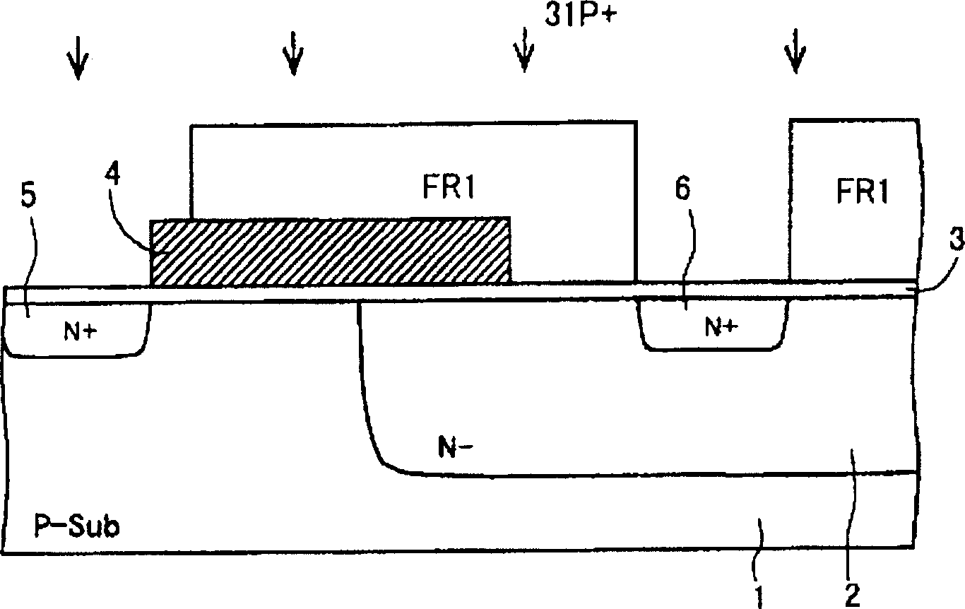
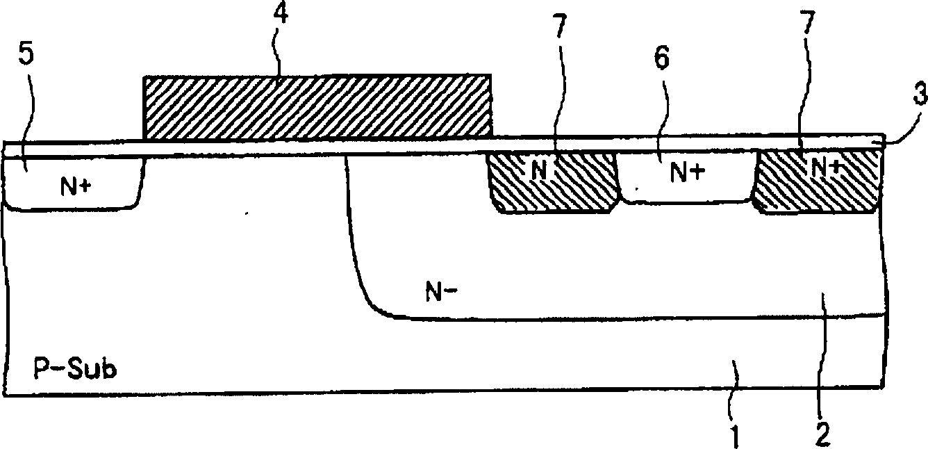
[0043] exist image 3 In the semiconductor device according to the first embodiment of the present invention, a gate insulating film 3 is formed on a semiconductor substrate of one conductivity type, for example, a P-type semiconductor substrate 1, and a gate electrode 4 is formed through the gate insulating film 3. . Moreover, a high-concentration reverse conduction (N+) type source region 5 is formed so as to be adjacent to one end of the gate electrode 4, and a low-concentration N+ type source region 5 is formed opposite to the above-mentioned source region 5 through the channel region under the gate electrode 4 The reverse conduction (N-) type drain region 2, moreover, has also formed the reverse conduction (N+) type drain region 6 of high concentration, makes it leave the other end of above-mention...


PUM


Abstract

The object of the present invention is to improve the working withstand voltage. The semiconductor device of the present invention has: a gate electrode (4); a low-concentration N-type drain region (2) formed adjacent to the gate electrode; and an N+ type drain region (6) separated from the gate electrode (4). ) and is included in the above-mentioned low-concentration N-type drain region (2), characterized in that: a medium-concentration N-type layer (7A) is formed, which is at least from the above-mentioned gate electrode (4) There is a position at a predetermined interval across the region between the above-mentioned high-concentration N+ type drain regions (6), and there is an impurity concentration peak at a position at a predetermined depth in the above-mentioned substrate (1), and in a region close to the substrate surface The impurity concentration becomes lower.

Description

technical field [0001] The present invention relates to a semiconductor device and its manufacturing method. More specifically, it relates to a technique for improving the operating withstand voltage characteristics of a high withstand voltage MOS transistor for a high power supply voltage (HV-VDD) used in an LCD driver or an EL driver, etc. . Background technique [0002] Hereinafter, regarding a semiconductor device related to a conventional example, while referring to Figure 12 The cross-sectional view of the LDD type high withstand voltage MOS transistor shown in . [0003] exist Figure 12 In this case, a gate electrode 53 is formed on a P-type semiconductor substrate (P-Sub) 51 via a gate insulating film 52 . Moreover, an N+ type source region 54 is formed so as to be adjacent to one end of the above-mentioned gate electrode 53, an N-type drain region 56 is formed opposite to the above-mentioned source region 54 via a channel region 55, and an N+ type drain region 57...

Claims


Application Information

Patent Timeline
Patent Type & Authority Patents(China)
IPC IPC(8): H01L29/78H01L21/336H01L21/265
CPCH01L21/26586H01L29/66659H01L29/7835H01L29/78
Inventor 菊地修一西部荣次铃木琢也
Owner SANYO ELECTRIC CO LTD
Learn More