
Semiconductor devices

A semiconductor and circuit technology, applied in the field of semiconductor devices with balanced circuits, can solve the problems of increased dispersion of high-frequency characteristics, deviation of high-power amplifier characteristics, and large alignment error.

Inactive Publication Date: 2006-11-29
MURATA MFG CO LTD
View PDF2 Cites 0 Cited by
  • Summary
  • Abstract
  • Description
  • Claims
  • Application Information

AI Technical Summary

Problems solved by technology

[0010] However, in the above-mentioned conventional push-pull type high-power amplifier, since most of the circuit components are formed on the PCB substrate 1, there are problems of increased device size and weight, and increased cost.
In addition, since the chip components and the like are mounted on the wiring with solder, there is a problem that the alignment error is large and the dispersion of high-frequency characteristics (RF characteristics) increases.
Especially in the matching circuit section composed of the choke coil L and the capacitor C at the part from the balun to the package leads, when the position of the chip capacitance section 9 (capacitor C) deviates, equivalently When the value of the choke coil L changes, the matching will deviate. As a result, there is a problem that the characteristics of the high-power amplifier will deviate greatly.

Method used


Image

  • Semiconductor devices
  • Semiconductor devices
  • Semiconductor devices

Examples


Embodiment 1

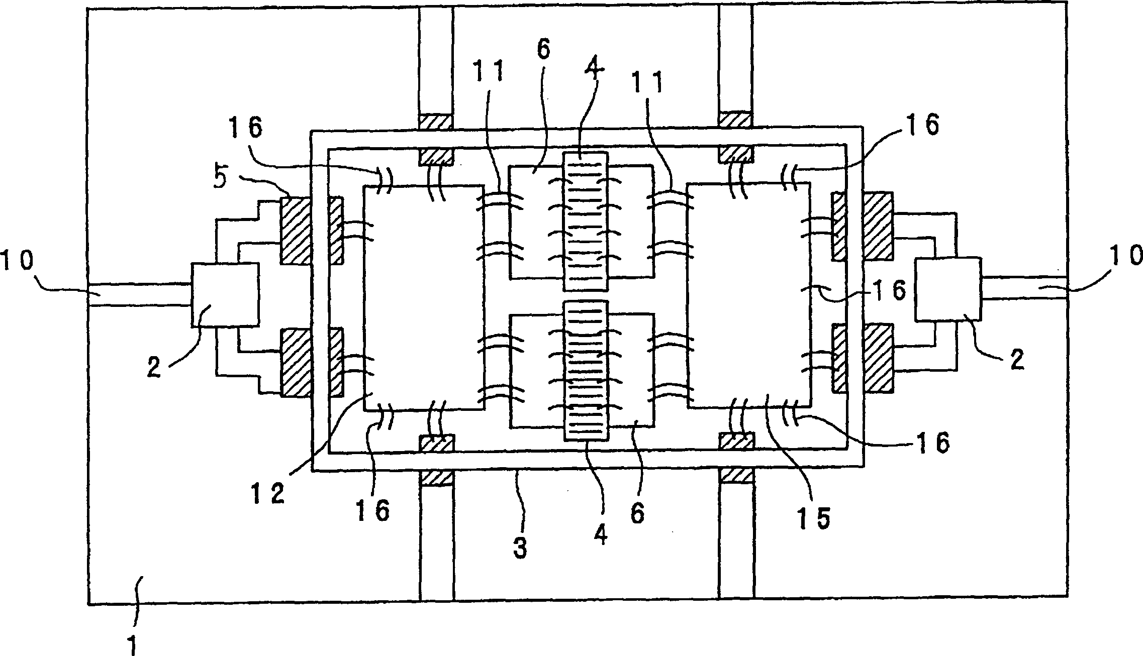
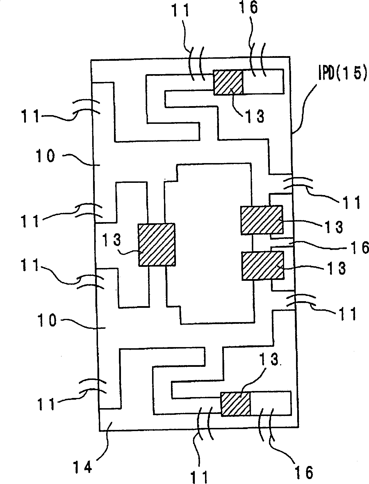
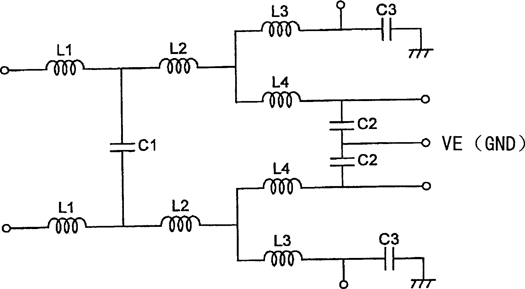
[0031] Below, refer to Figure 1 to Figure 3 Example 1 of the present invention will be described. figure 1 is a plan view showing a semiconductor device according to Embodiment 1 of the present invention, figure 2 is the top view of the balanced matching circuit on the output side, image 3 is its equivalent circuit diagram.

[0032] The configuration example shown in the figure explains the case of using a push-pull type high-power amplifier, which is mainly used in the high-frequency band of 0.8 to 2.4 GHz. Reference numeral 1 in the figure is a housing of a PCB substrate (insulating substrate) on which circuit components are mounted. 2 is a balanced-unbalanced converter (balun), which is a passive distributed constant circuit used for connection (conversion) from a balanced line to an unbalanced line or a connection (conversion) opposite thereto. 3 is a package, and 4 is a semiconductor chip for high-frequency amplification, each of which is composed of a field effec...

Embodiment 2

[0048] Below, refer to Figure 7 and Figure 8 , to illustrate Embodiment 2 of the present invention. Figure 7 It is a plan view showing the output side IPD of the semiconductor device according to Embodiment 2 of the present invention, Figure 8 is the equivalent circuit diagram. In Embodiment 1, the matching circuit is composed of series connected L1, L2, L3 and grounding capacitors C1 and C2. In this embodiment 2, the matching circuit is composed of series connected capacitor C4 and grounding inductor L5, and the inductor L5 is connected to Between two channel matching circuits.

[0049] exist Figure 7 and Figure 8 In the shown configuration, since the upper circuit and the lower circuit have a phase difference of 180 degrees, a balanced circuit is used, and the midpoint of the inductor L5 connecting the two matching circuits becomes a virtual ground point, and operates as if half of the inductance of L5 is grounded. Therefore, it becomes ideal grounding in a high ...

Embodiment 3

[0053] Below, refer to Figure 9 to Figure 11 Embodiment 3 of the present invention will be described. Figure 9 is a top view of a semiconductor device according to Embodiment 3 of the present invention, Figure 10 is a top view of an IPD with a built-in balun on its output side, Figure 11 yes means Figure 10 The diagram of the equivalent circuit diagram is shown.

[0054] In this embodiment 3, in Figure 9 to Figure 11 Among them, 20 is an IPD with a built-in balun on the input side, and 21 is an IPD with a built-in balun on the output side. On the input side and the output side, the balun 2 is included in the IPD20 respectively. and structures in IPD21.

[0055] In this way, by forming the balun 2 on the substrate in the IPD, it is possible to further reduce the size and weight of the semiconductor device and reduce the cost compared to the case of the first embodiment. In addition, with the above-mentioned structure, it is not necessary to directly arrange the balu...


PUM


Abstract

A semiconductor chip for amplification is connected between input-side and output-side matching circuits, and each of matching circuits includes balanced circuits which receive signals different in phase by 180 degrees, divided from an input signal. The balanced circuits are connected at a virtual grounding point, which is used as a grounding point sensitive to RF characteristics in an IPD. Thus, a semiconductor device can be free from influence of variations of grounding wires and can be reduced in size, weight, and cost.

Description

technical field [0001] The present invention relates to a semiconductor device, in particular to a semiconductor device with a balanced circuit used in a high frequency band above 800 MHz. Background technique [0002] Now, as a semiconductor device in which a plurality of IC chips are mounted in one package, in order to obtain electrical connection between the IC chips, a relay electrode portion is provided in the middle, and the electrical connection between the IC chips is performed through the relay electrode portion. At the same time as the connection, the connection with the outside is also carried out. The relay electrode part is arranged on the insulating substrate in a symmetrical shape, fixed on the surface of the insulating substrate and various circuit patterns are formed, and various circuit patterns are connected and mounted on each circuit pattern with solder. a semiconductor chip. [0003] As a conventional high-frequency-high-output semiconductor device, fo...

Claims


Application Information

Patent Timeline
Patent Type & Authority Patents(China)
IPC IPC(8): H03F3/60H01L23/50H01L23/525H01L23/538H01L23/12H01L23/66H03F1/56
CPCH01L2924/01014H01L24/48H01L23/66H01L2924/30105H01L2924/014H01L2924/19042H01L2924/0105H01L2224/49111H01L2924/19011H01L2924/01072H01L2924/01005H03F3/602H01L2924/01033H01L2924/01075H01L2924/01082H01L2223/6644H01L2924/01004H01L2924/3011H01L2224/49175H01L2224/48091H01L2924/10253H01L24/49H01L2924/19041H01L2924/01006H01L2924/19043H01L2924/14H03F1/565H01L2924/01068H01L2924/30107H01L2924/1306H01L2924/1305H01L2224/451H01L2924/30111H01L2924/00014H01L24/45H01L2924/181H01L2924/00H01L2224/05599
Inventor 井上晃太田彰后藤清毅
Owner MURATA MFG CO LTD
Learn More