

Flexible circuit board
A flexible circuit board and circuit technology, used in printed circuits, electrical components, cooling/ventilation/heating transformation, etc., to increase heat dissipation efficiency, improve connection reliability, and increase heat dissipation area.
- Summary
- Abstract
- Description
- Claims
- Application Information
AI Technical Summary
Problems solved by technology
Method used
Image

Examples
Embodiment 1
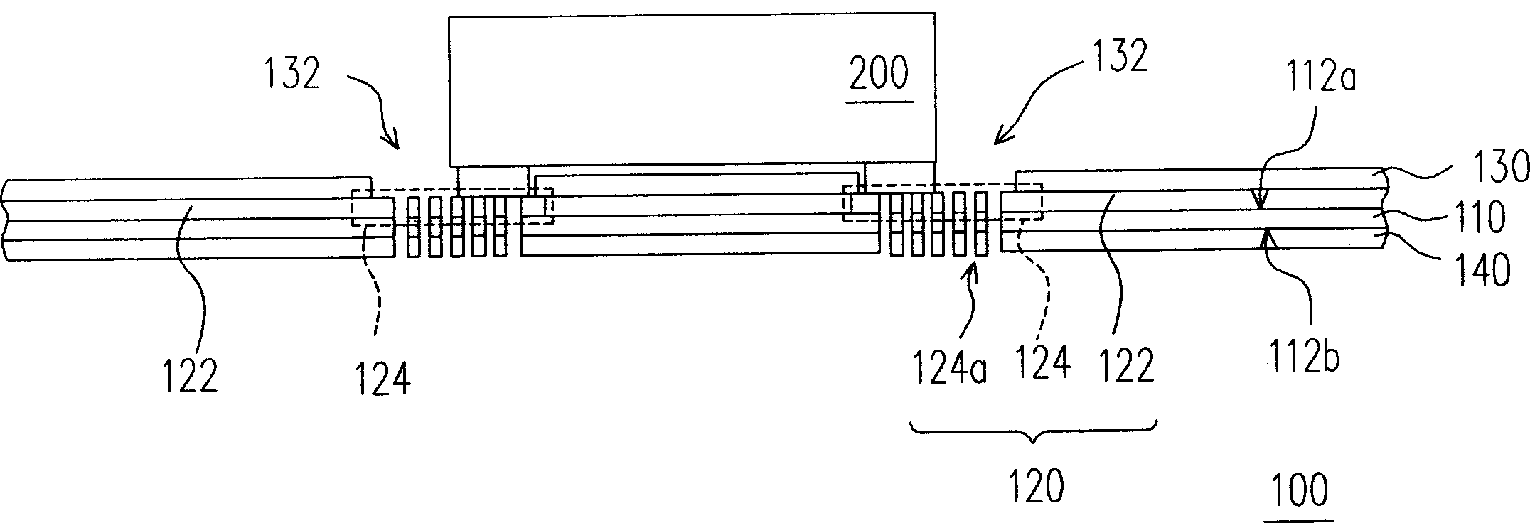
[0066] see figure 1As shown, it is a schematic cross-sectional view of a flexible circuit board according to the first preferred embodiment of the present invention. The flexible circuit board 100 of the present invention is suitable for carrying at least one electronic component 200, and the electronic component 200 is connected with the flexible circuit board 100, and the electronic component 200 is such as a light emitting diode component or an organic electroluminescence component. The flexible circuit board 100 includes, for example, a first insulating layer 110 , a patterned metal layer 120 , a second insulating layer 130 and a plurality of first thermal vias 124 a. Wherein, the first insulating layer 110 has a first surface 112a and a second surface 112b corresponding to the first surface 112a, and the material of the first insulating layer 110 is, for example, polyimide or other transparent insulating materials. . The patterned metal layer 120 is disposed on the firs...
Embodiment 2
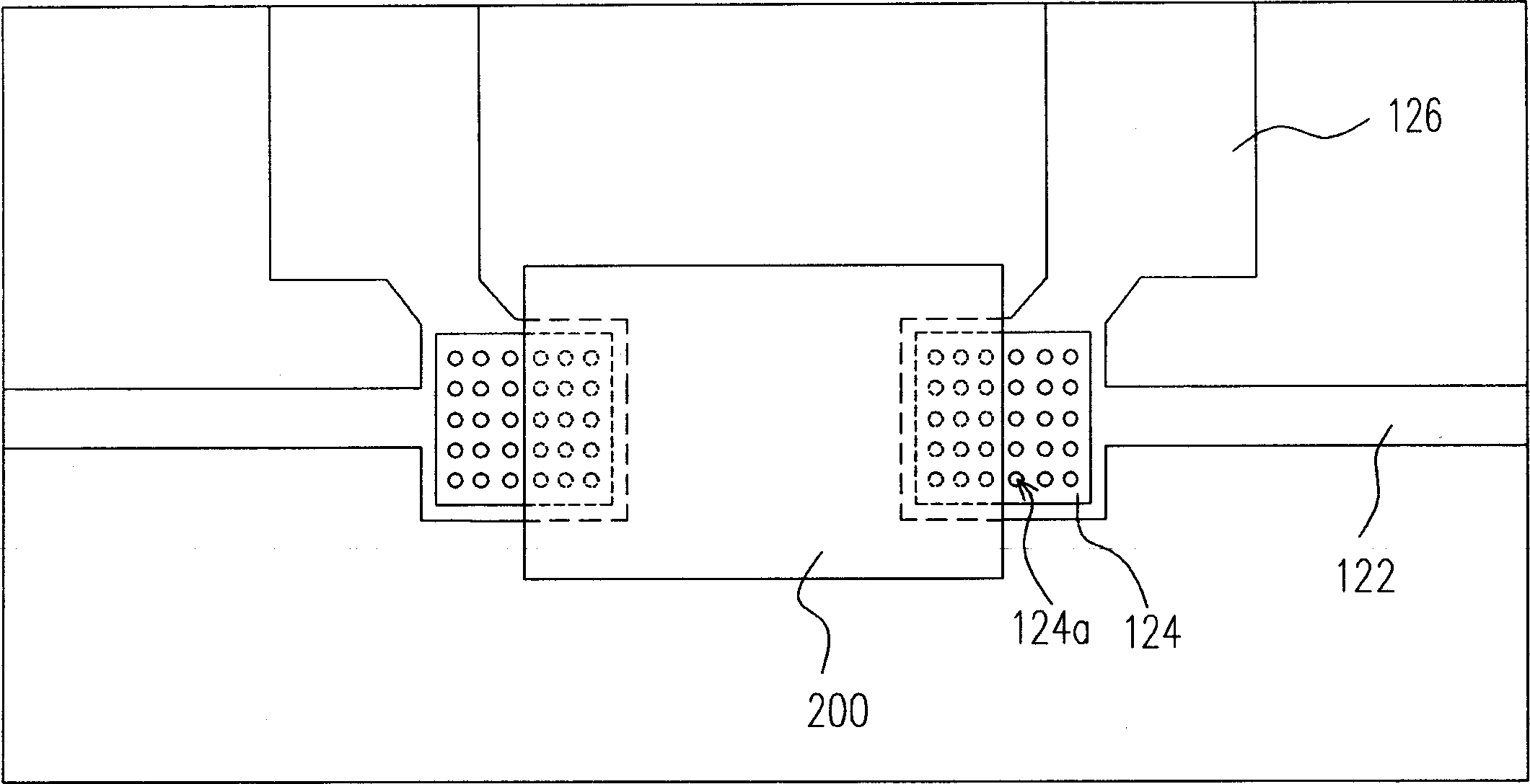
[0071] see figure 2 As shown, it is a schematic top view of a flexible circuit board according to the second preferred embodiment of the present invention. This embodiment is similar to the first embodiment, but the difference is that this embodiment has a first heat dissipation pad 126, and the first heat dissipation pad 126 is connected with the connection pad 124 to increase the overall heat dissipation area, wherein the first heat dissipation pad 126 The pad 126 is made of copper, aluminum or other materials with good electrical and thermal conductivity. Therefore, the connection pad 124 can conduct part of the heat energy to the first heat dissipation pad 126 , and conduct it to the outside through the first heat dissipation pad 126 , so as to reduce the temperature of the connection pad 124 .
Embodiment 3
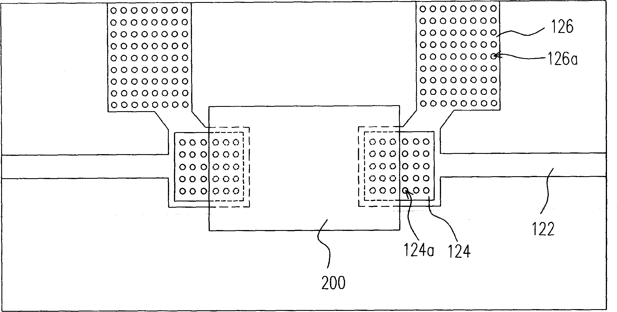
[0073] see image 3 Shown is a schematic top view of a flexible printed circuit board according to the third preferred embodiment of the present invention, please also refer to figure 1 and image 3 As shown, this embodiment is similar to the second embodiment, but the difference is that: the flexible circuit board 100 of this embodiment has a plurality of second heat conduction vias 126a, and the second heat conduction vias 126a are located on the first heat dissipation pad 126 , wherein the second thermal via 126 a penetrates through the first insulating layer 110 , the patterned metal layer 120 , the second insulating layer 130 and the heat dissipation metal film 140 . Therefore, the above-mentioned second heat conduction vias 126 a can also increase the heat dissipation area of the first heat dissipation pad 126 , thereby increasing the heat dissipation efficiency of the first heat dissipation pad 126 , so as to achieve the purpose of the present invention.
PUM
 Abstract
Description
Claims
Application Information