Method of processing semiconductor wafers to build in back surfact demage

A semiconductor and rear surface technology, applied in semiconductor/solid-state device manufacturing, machine tools suitable for grinding workpiece planes, grinding devices, etc., can solve problems affecting wafer flatness and high cost

Inactive Publication Date: 2002-01-09
MEMC ELECTONIC MATERIALS INC
View PDF0 Cites 10 Cited by
  • Summary
  • Abstract
  • Description
  • Claims
  • Application Information

AI Technical Summary

Problems solved by technology

This additional processing can seriously affect the flatness of the wafer
Additional steps are costly due to increased workmanship and handling, requiring special precautions to protect the front surface from damage

Method used


Image

  • Method of processing semiconductor wafers to build in back surfact demage
  • Method of processing semiconductor wafers to build in back surfact demage
  • Method of processing semiconductor wafers to build in back surfact demage

Examples


example

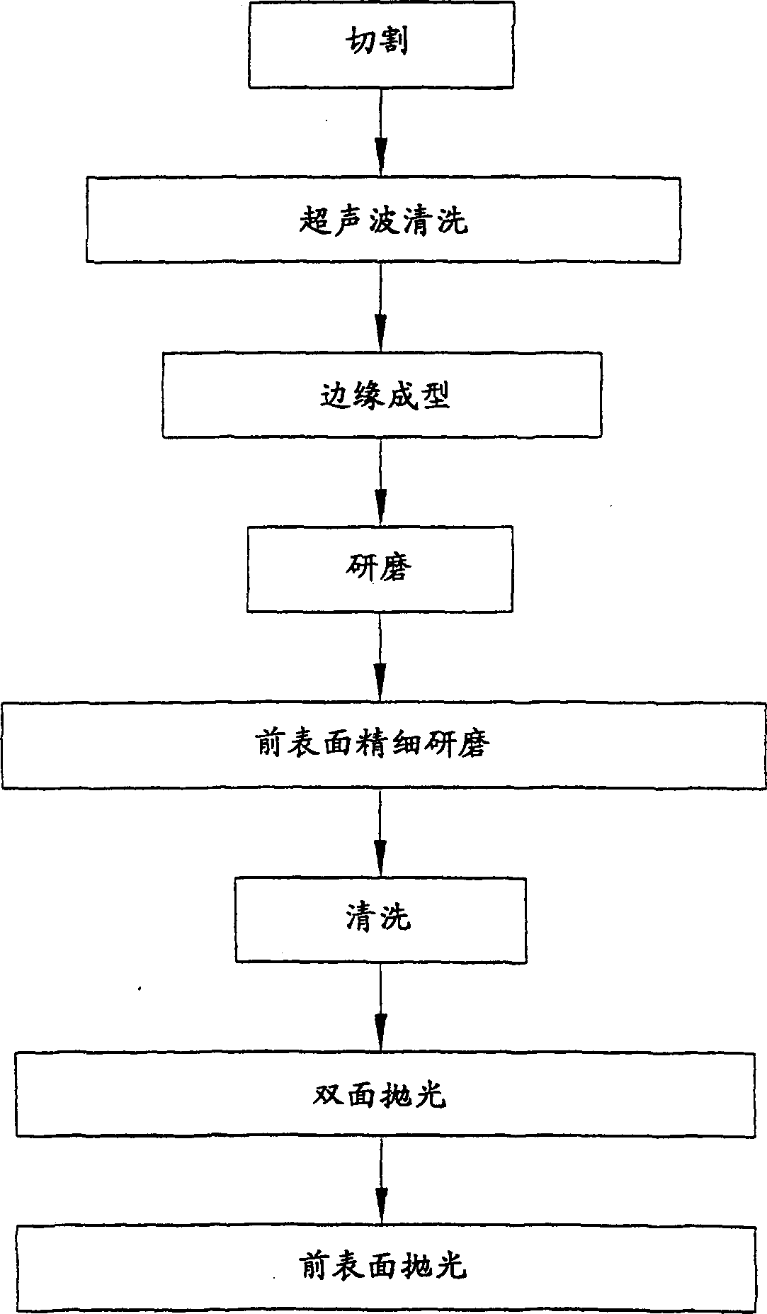
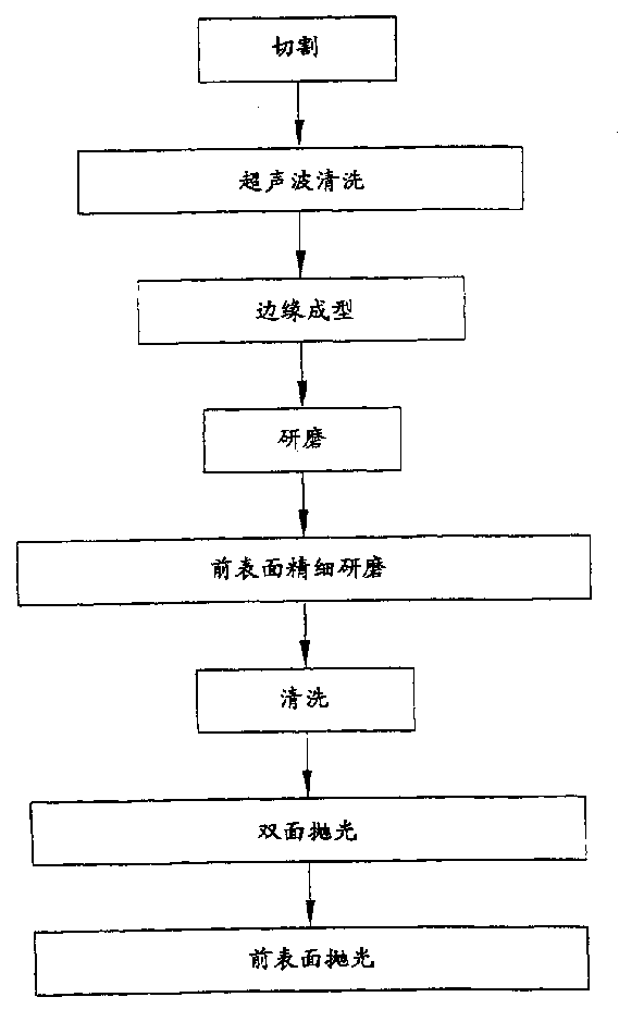
[0027] according to figure 1 Fifteen silicon semiconductor wafers having a diameter of 200 mm were processed as shown and as described in the first embodiment. The grinding operation was performed using a 15 μm particle grinding slurry, removing approximately 80 microns (40 microns on each of the front and rear surfaces) of material from each wafer. A fine grinding operation was then performed on the front surface of each wafer to remove a thickness of 15-17 microns from the wafer. Each wafer was then subjected to a DSP operation in which approximately 5-6 microns were removed from the wafer, with approximately equal amounts removed from the front and rear surfaces. After the DSP operation, the OISF count on the rear surface of one wafer was measured to be 20000 / cm2.

no. 2 example

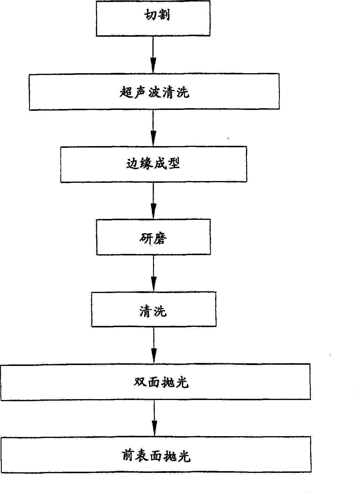
[0029] exist figure 2 In the second embodiment of the invention shown, the fine grinding step is omitted. In this second embodiment, cutting, ultrasonic cleaning, edge shaping and grinding are performed as described in the first embodiment. Only the abrasive used in the grinding equipment is preferably between about 5-10 microns. Smaller dimensions are preferred because there is less damage to the surface, which reduces the amount of wafer material that must be removed during the DSP process. The wafer is then cleaned and subjected to a DSP process similar to that described in the first embodiment, except that more material is removed from the front surface than from the rear surface.

[0030] The DSP process of the second embodiment preferably removes almost all damage from the front surface while leaving some amount of damage on the rear surface. Damage sites on the rear surface contribute to gettering of the rear surface. The DSP device can be set to remove a significa...


PUM


Abstract

A method of processing a semiconductor wafer sliced from a single-crystal ingot includes lapping front and back surfaces of the wafer to reduce the thickness of the wafer and to improve the flatness of the wafer. The front surface is subjected to fine grinding to reduce the damage on the front surface while leaving damage on the back surface intact. The front and back surfaces are simultaneously polished to improve the flatness of the wafer and to reduce wafer damage on the front and back surfaces. The wafer damage remaining on the back surface is greater than the wafer damage on the front surface. The wafer damage remaining on the back surface facilitates gettering.

Description

Background of the invention [0001] The present invention relates generally to semiconductor wafer processing methods, and more particularly to such a semiconductor wafer processing method for producing relatively flat wafers with rear surface damage for external gettering. [0002] Semiconductor wafers are typically prepared from single crystal ingots, such as silicon ingots, which are trimmed and ground to have one or more flats for proper orientation of the wafers in subsequent processing. The ingot is then cut into individual wafers, which are subjected to various processes to reduce wafer thickness, remove damage from the cutting operation, and create highly reflective surfaces. Typically, the peripheral edge of each wafer is rounded to reduce the risk of damage to the wafer during further processing. A lapping operation (abrasive slurry treatment) is then performed on the front and rear surfaces of the wafer to reduce the thickness of the wafer and remove damage caused b...

Claims


Application Information

Patent Timeline
Patent Type & Authority Applications(China)
IPC IPC(8): B24B7/22B24B37/00H01L21/304H01L21/306
CPCH01L21/02008H01L21/02013H01L21/02024H01L21/304
Inventor 辛云彪
Owner MEMC ELECTONIC MATERIALS INC
Why Eureka
Try Eureka