Check patentability & draft patents in minutes with Patsnap Eureka AI!

Chip heat sink package structure and making method thereof

A packaging structure and chip heat dissipation technology, which is applied in the direction of cooling/ventilation/heating transformation, semiconductor/solid-state device manufacturing, electrical components, etc., can solve the problems of reduced heat dissipation effect, increasing the gap between the supporter and the die, and difficulty in implementation. To achieve the effect of easy implementation

Inactive Publication Date: 2002-10-02
VIA TECH INC
View PDF1 Cites 7 Cited by
  • Summary
  • Abstract
  • Description
  • Claims
  • Application Information

AI Technical Summary

Problems solved by technology

[0006] The technical problem to be solved by the present invention is to provide a chip heat dissipation packaging structure, which can solve the problems of implementation difficulties in the known technology and the need to increase the gap between the supporter and the die due to packaging problems, resulting in reduced heat dissipation and other deficiencies.

Method used


Image

  • Chip heat sink package structure and making method thereof
  • Chip heat sink package structure and making method thereof
  • Chip heat sink package structure and making method thereof

Examples


Embodiment Construction

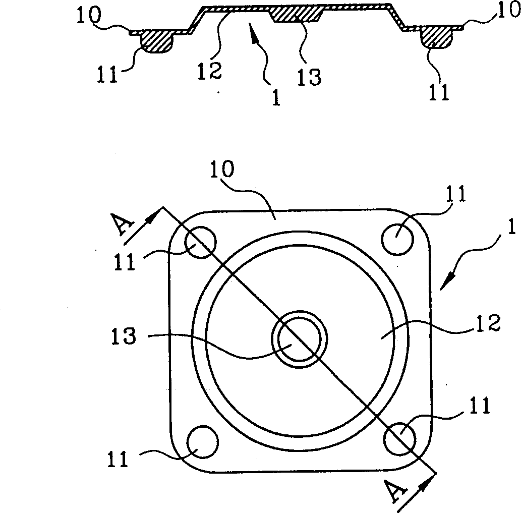
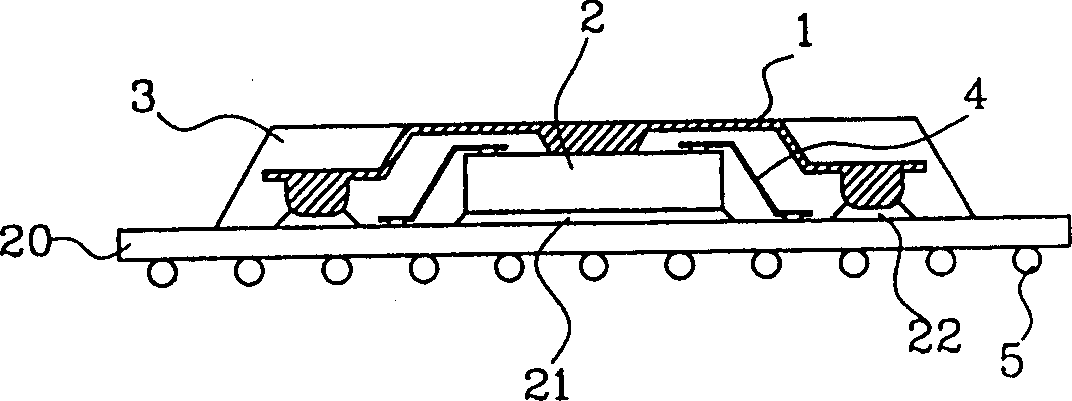
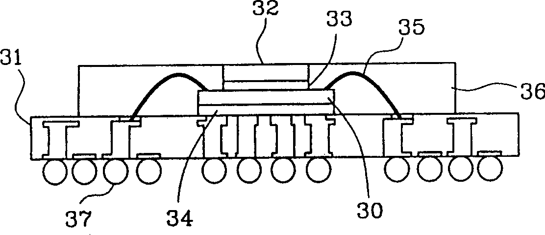
[0038] image 3 Shown is a schematic cross-sectional view of the structure of the first embodiment of the present invention. The chip heat dissipation packaging structure of the present invention is to improve the ability of the chip to dissipate heat through the setting of a heat sink 32 in a chip package. It includes: a substrate 31, by The substrate 31 carries a die 30 cut from a wafer, and the die 30 is pasted on the proper position of the substrate 31 through a second thermally conductive adhesive 34 of a suitable material between the die 30 and the substrate 31, and then after a period of time The second heat-conducting adhesive 34 is cured so that the die 30 can be fixed at an appropriate position on the substrate 31; afterward, the signal input and output terminals on the die 30 are connected to the appropriate contacts on the substrate 31 by wires 35 of appropriate materials ; This tube core 30 is the core of semiconductor work. When performing calculation processing,...


PUM


Abstract

This invention relates to a chip heat sink packaging structure and its method of production, containing a substrate, a transistor core set on the substrate, a heat sink and a sealing gel material with the characteristic of the heat sink to be a sheet shape set on the said transistor core and be adhered together by the first heat conducting gel which is put on said substrate, transistor core and side radiating sheet. The production method is to cut the wafer to get the core chip to be adhered to a substrate by a heat conducting gel which will fix said core on said substrate after solidification then to be adhered and fixed by another heat conducting gel, and pulled with wire, adhered and welded with tin ball to finish the work to radiate the heat of the core to outside quickly due to the direct adhering of the radiator and the core.

Description

technical field [0001] The invention relates to a chip packaging structure and a manufacturing method thereof, in particular to a chip packaging structure including a heat dissipation device and a manufacturing method thereof. Background technique [0002] The continuous improvement and development of integrated circuits, the continuous reduction in volume, the continuous decline in prices, and the continuous improvement of functions, while improving functions, the core of integrated circuit work, the manufacturing process of semiconductor dies is becoming more and more rigorous and important; When the semiconductor die is working, the calculation and processing performed in such a small space will generate a relatively large amount of heat, and the generated heat must be dissipated in an appropriate way to avoid overheating of the integrated circuit chip Errors in calculation processing can cause damage to hardware circuits in severe cases. Therefore, the work of heat trea...

Claims


Application Information

Patent Timeline
IPC IPC(8): H01L21/50H01L23/34H05K7/20
CPCH01L2224/48091H01L2224/48247H01L2224/73215H01L2224/73265
Inventor 许志行
Owner VIA TECH INC
Features
  • R&D
  • Intellectual Property
  • Life Sciences
  • Materials
  • Tech Scout
  • Unparalleled Data Quality
  • Higher Quality Content
  • 60% Fewer Hallucinations
Learn More