Non-volatibility semiconductor memory

A non-volatile, semi-conductive technology, applied in semiconductor devices, static memory, semiconductor/solid-state device manufacturing, etc., can solve problems such as working speed and wrong work

Inactive Publication Date: 2002-11-20
RENESAS ELECTRONICS CORP
View PDF0 Cites 0 Cited by
  • Summary
  • Abstract
  • Description
  • Claims
  • Application Information

AI Technical Summary

Problems solved by technology

[0029] The present invention is completed in order to solve these problems, and its purpose is to obtain and can realize suppressing or avoiding the generation of the interference defect phenomenon when erasing, suppress the decline of the operating speed of the memory cell transistor that the high resistance of factor bit line causes and avoid Non-volatile semiconductor memory that malfunctions of memory cell transistors due to downsizing of windows

Method used


Image

  • Non-volatibility semiconductor memory
  • Non-volatibility semiconductor memory
  • Non-volatibility semiconductor memory

Examples


Embodiment 1

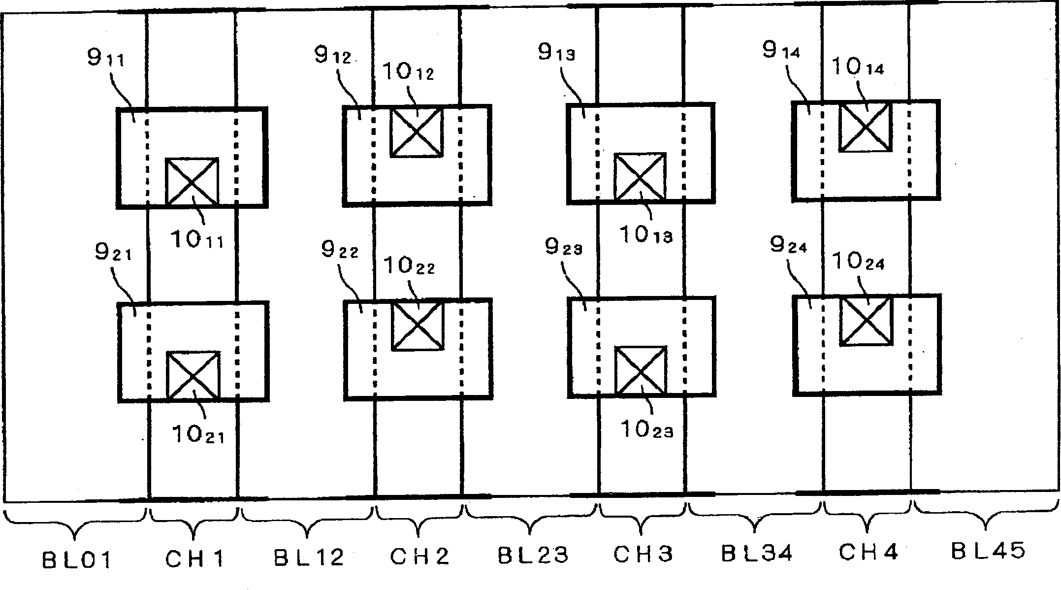
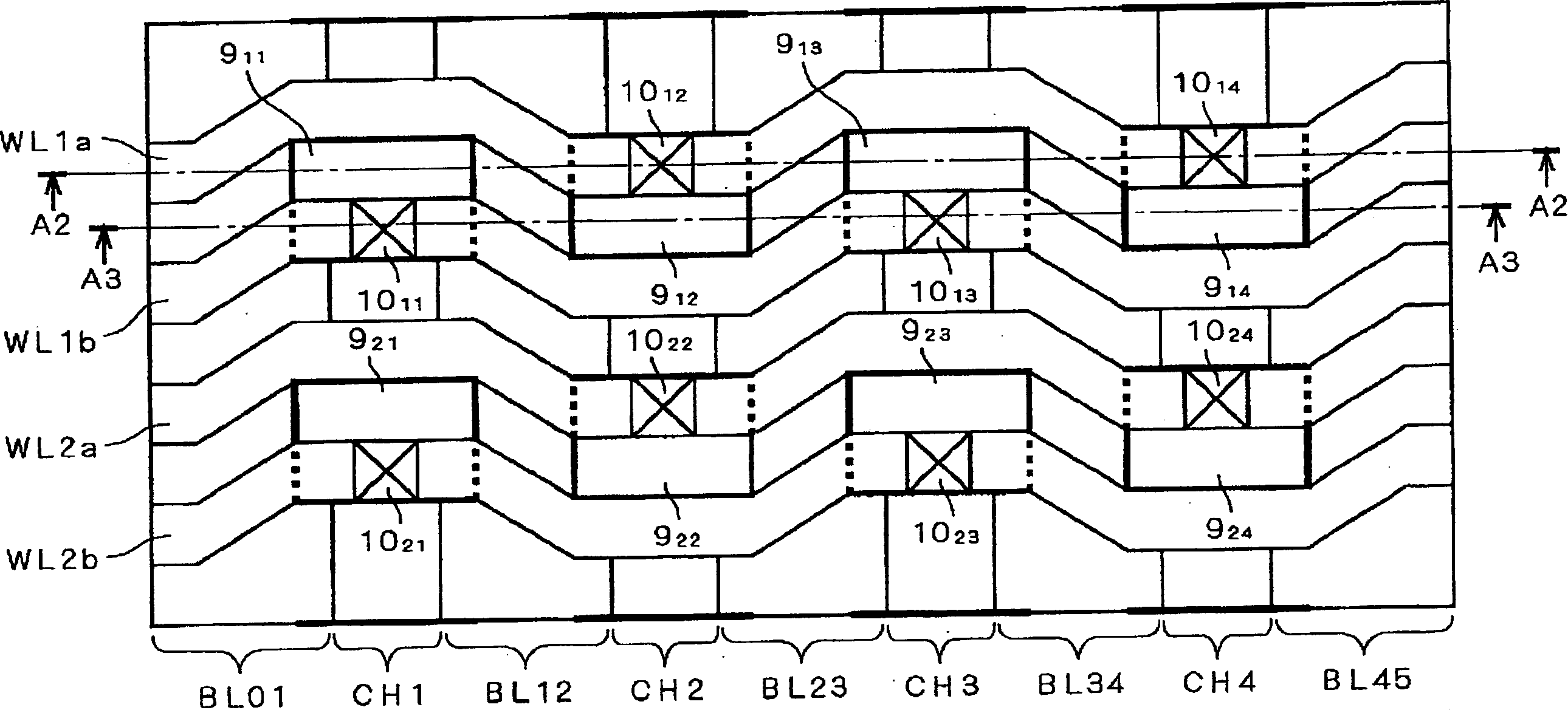
[0116] figure 1 It is a plan view schematically showing the structure of the nonvolatile semiconductor memory according to Embodiment 1 of the present invention. A nonvolatile semiconductor memory includes a memory cell array portion in which a plurality of memory cell transistors are formed in a matrix in a semiconductor substrate. figure 1 In , the structure of a part of the above-mentioned memory cell array unit is extracted and shown. In addition, in figure 1 In , description of word lines is omitted. bit line BL (at figure 1 In , codes BL01, BL12, BL23, BL34, BL45) are formed extending in the column direction of the above-mentioned matrix.

[0117] Channel region CH (in figure 1 , denoted by symbols CH1 to CH5) are formed extending between adjacent bit lines BL in the column direction. A gate electrode 9 is formed on the channel region CH (in figure 1 , marked with symbol 9 11 ~9 14 ,9 21 ~9 24 ). Gate electrode 9 11 ~9 14 and 9 21 ~9 24 are the gate...

Embodiment 2

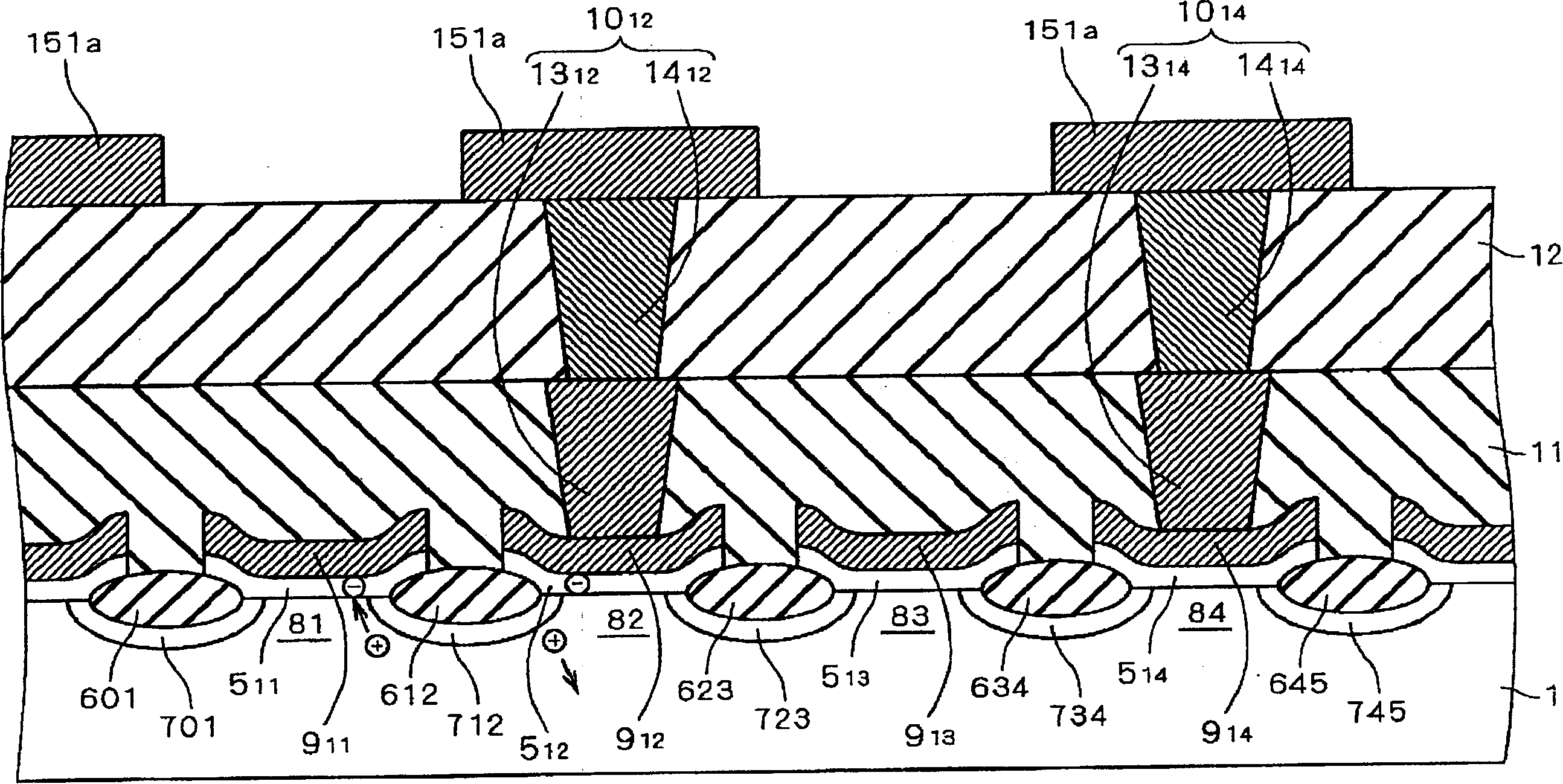
[0142] Figure 25 It is a plan view schematically showing the structure of the nonvolatile semiconductor memory according to Embodiment 2 of the present invention. In addition to the nonvolatile semiconductor memory described in the description of the prior art, the nonvolatile semiconductor memory of the present embodiment 2 (refer to Figure 61 , 62 ), also has metal wiring ML (in Figure 25 , marked with symbols ML01, ML12, ML23, ML34, ML45) and bolt 20. The metal lines ML are formed to extend in the column direction corresponding to the bit lines BL. In addition, metal wiring ML is connected to bit line BL via plug 20 .

[0143] Figure 26 is shown along with Figure 25 The sectional view of the sectional structure related to the position of the line A4-A4 shown in . and Figure 25 The conductive film 9 corresponding to the word lines WL1 and WL2 has a structure in which a doped polysilicon film 25 , a tungsten silicide film 26 , a tungsten nitride film 27 and a tun...

Embodiment 3

[0160] Figure 34 It is a cross-sectional view showing the structure of a memory cell transistor related to the nonvolatile semiconductor memory according to Embodiment 3 of the present invention. A polysilicon film 51 is formed in a gate insulating film 50 made of a silicon oxide film. Under the element isolation insulating film 6, impurity diffusion regions 7 functioning as source and drain regions of memory cell transistors are formed. Polysilicon film 51 is formed only in the end portion of gate insulating film 50 close to impurity diffusion region 7 . The polysilicon film 51 functions as a floating gate of the memory cell transistor, and can store electrons inside.

[0161] Writing is performed by injecting hot electrons into the polysilicon film 51 . Erasing is performed by injecting hot holes induced by the interband tunneling current into the polysilicon film 51 . Reading is performed by monitoring the leakage current or the leakage voltage and detecting the thresh...


PUM


Abstract

It is an object of the present invention to obtain a nonvolatile semiconductor memory capable of suppressing the occurrence of disturbing defects during erasing. Bit lines BL are formed extending in the column direction of the matrix. Gate electrode 9 is formed on channel region CH. The nonvolatile semiconductor memory includes a plug 10 for interconnecting the gate electrode 9 and the word line. Each row of word lines has two sub-word lines WL. Sub-word lines WL1a, WL1b and sub-word lines WL2a, 2b are sub-word lines belonging to the same row, respectively. The sub-word line WL1a is in contact with the plugs 1012 and 1014, the sub-word line WL1b is in contact with the plugs 1011 and 1013, the sub-word line WL2a is in contact with the plugs 1022 and 1024, and the sub-word line WL2b is in contact with the plugs 1021 and 1023.

Description

[0001] [Detailed description of the invention] (1) Technical field [0002] The present invention relates to nonvolatile semiconductor memories, and more particularly to the structure of NROM (Nitride Read Only Memory) type nonvolatile semiconductor memories. (2) Background technology [0003] Figure 61 It is a plan view showing part of the structure of a conventional NROM-type nonvolatile semiconductor memory. But when Figure 61 In FIG. 2 , the arrangement relationship between the word lines WL1 and WL2 , the bit lines BL1 and BL2 and the channel regions CH1 to CH3 is only schematically shown. Word lines WL1 and WL2 are formed extending in a predetermined direction (hereinafter referred to as “row direction”). The bit lines BL1 and BL2 are formed to extend in a direction perpendicular to the row direction (hereinafter referred to as "column direction"). Channel regions CH1 to CH3 are formed to extend in the column direction between adjacent bit lines. [0004] Figure...

Claims


Application Information

Patent Timeline
Patent Type & Authority Applications(China)
IPC IPC(8): G11C16/06G11C16/02G11C16/04H01L21/76H01L21/8246H01L21/8247H01L27/10H01L27/115H01L29/788H01L29/792
CPCG11C16/0475H10B43/30H10B69/00H10B41/30H01L29/788H10B99/00
Inventor 国清辰也
Owner RENESAS ELECTRONICS CORP
Why Eureka
Try Eureka