

Semiconductor device and its manufacture
A manufacturing method and semiconductor technology, applied in semiconductor/solid-state device manufacturing, transistors, electrical components, etc., can solve problems such as reducing and reducing carrier mobility
- Summary
- Abstract
- Description
- Claims
- Application Information
AI Technical Summary
Problems solved by technology
Method used
Image

Examples
Embodiment 1
[0088] [A-1. Manufacturing method]
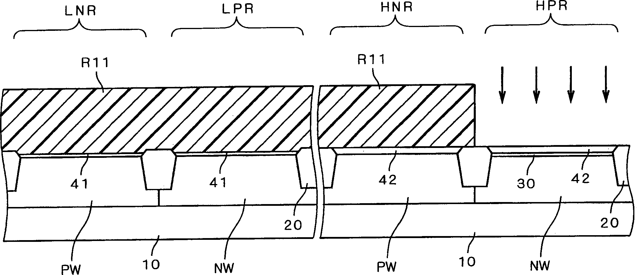
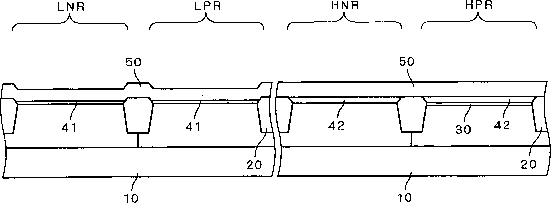
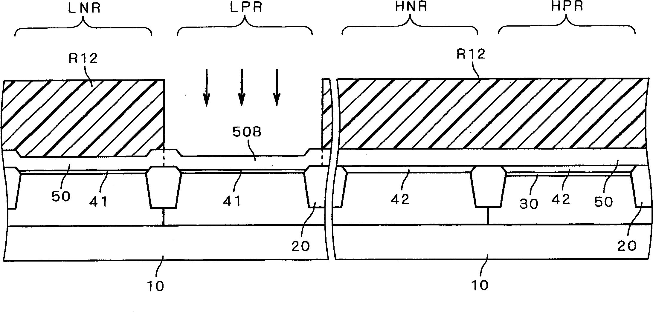
[0089] A method of manufacturing a semiconductor device having a CMOS transistor 100A and a CMOS transistor 100B as a method of manufacturing a semiconductor device according to Embodiment 1 of the present invention will be described with reference to FIGS. 1 to 9 . The structures of the CMOS transistor 100A corresponding to the low voltage and the CMOS transistor 100B corresponding to the high voltage are shown in the section explaining the final process. Figure 9 middle.
[0090] First, as shown in FIG. 1, an element isolation insulating film 20 is selectively formed in the surface of a silicon substrate 10, and a low-voltage NMOS region LNR and a low-voltage PMOS region LPR for forming a low-voltage NMOS transistor and a low-voltage PMOS transistor are defined. , specifying the high voltage NMOS region HNR and the high voltage PMOS region HPR forming the high voltage NMOS transistor and the high voltage PMOS transistor.
[0091] Corre...
Embodiment 2
[0120] [B-1. Manufacturing method]
[0121] A method of manufacturing a semiconductor device having a CMOS transistor 200A and a CMOS transistor 200B as a method of manufacturing a semiconductor device according to Embodiment 2 of the present invention will be described with reference to FIGS. 10-13. The structures of the CMOS transistor 200A corresponding to the low voltage and the CMOS transistor 200B corresponding to the high voltage are shown in the section explaining the final process. Figure 13 middle. with Figure 1- Figure 9 Structures having the same manufacturing methods of the low-voltage corresponding CMOS transistor 100A and the high-voltage corresponding CMOS transistor 100B described above are assigned the same reference numerals, and repeated explanations are omitted.
[0122] First, as shown in FIG. 10, a gate insulating film 41 is formed on the entire surface of the low-voltage NMOS region LNR and the low-voltage PMOS region LPR on the silicon substrate 10 t...
Embodiment 3
[0145] [C-1. Manufacturing method]
[0146] use Figure 14-21 A method of manufacturing a semiconductor device having a CMOS transistor 300A and a CMOS transistor 300B as a method of manufacturing a semiconductor device according to Embodiment 3 of the present invention will be described. The structures of the CMOS transistor 300A corresponding to the low voltage and the CMOS transistor 300B corresponding to the high voltage are shown in the section explaining the final process. Figure 21 middle. with Figure 1- Figure 9 Structures having the same manufacturing methods of the low-voltage corresponding CMOS transistor 100A and the high-voltage corresponding CMOS transistor 100B described above are assigned the same reference numerals, and repeated explanations are omitted.
[0147] First, if Figure 14 1 and 2, a gate insulating film 41 is formed on the entire surface of the low voltage NMOS region LNR and the low voltage PMOS region LPR on the silicon substrate 10. Gate ...
PUM
| Property | Measurement | Unit |
|---|---|---|
| Thickness | aaaaa | aaaaa |
Abstract
Description
Claims
Application Information