

LED epitaxial wafer electroluminescent nondestructive detection method
A technology of light-emitting diodes and detection methods, which is applied in the field of detection instruments and can solve problems such as destructiveness and non-continuity
Inactive Publication Date: 2003-02-05
TSINGHUA UNIV
View PDF0 Cites 27 Cited by
- Summary
- Abstract
- Description
- Claims
- Application Information
AI Technical Summary
Problems solved by technology
So this detection method is destructive and not continuous
Method used
View moreImage
Smart ImageViewing Examples

Examples
Embodiment Construction
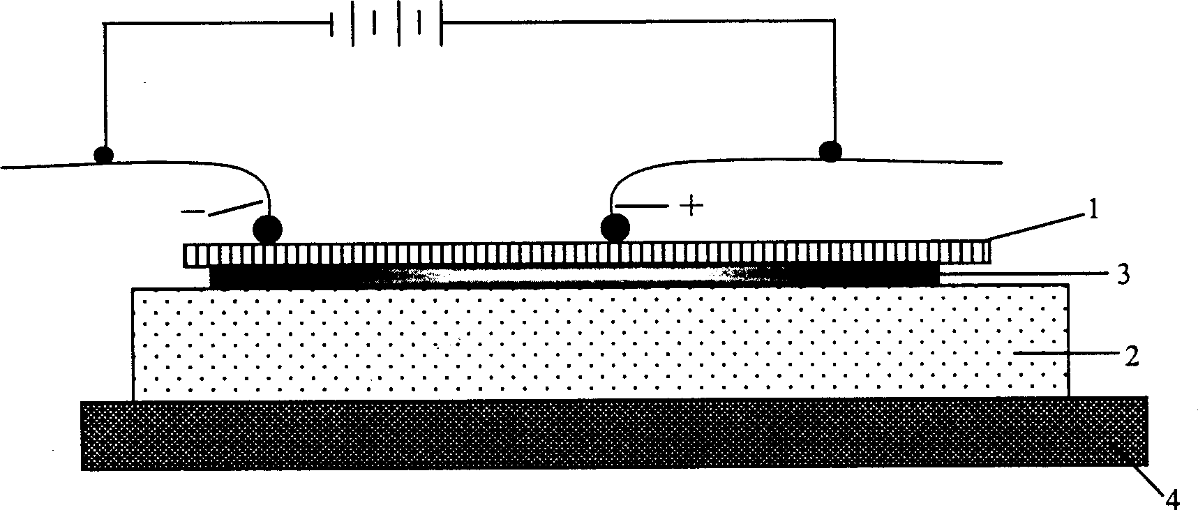
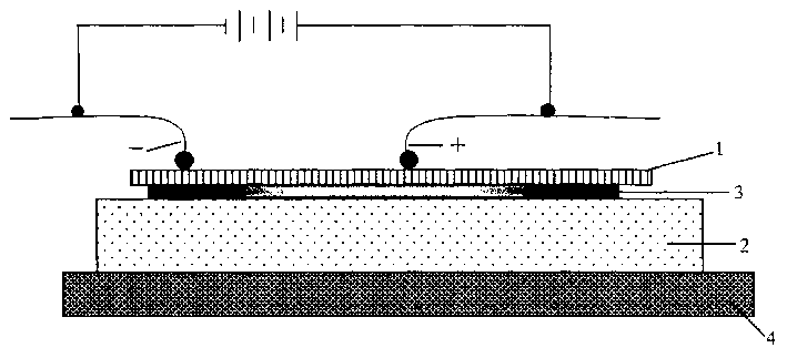
[0009] figure 1 Among them, 1 is the p-type layer, 2 is the n-type layer, 3 is the light-emitting layer, and 4 is the base. When testing, place positive and negative electrodes on the surface of the LED epitaxial wafer and add a high-voltage constant current source. Due to the breakdown of the reverse diode, the luminous condition of the measured point can be measured. After measuring a point, move the positive electrode, and the same method as above can continue to detect, and continuously move the positive electrode to measure the luminescence status of the entire LED epitaxial wafer.
Login to View More PUM
 Abstract
The invented method for testing the pitaxial wafer of the light emitting diode (LED) belongs to the area of the test instrument. The positive and negative electrodes are set upon the surface of the epitaxial wafer of LED. The high-voltage constant current source is connected to the positive and negative electrode, making the p type layer and the n type layer in the epitaxial wafer of LED form thebackward diode. The breakdown of the backward diode caused by the high-voltage makes the entire circuit turn on so as to trigger off the luminescence of the luminous layer of the epitaxial wafer of LED. Thus, the target of the test is reached. The method is direct, safe and convenient. Moreover, the electric parameters such as the forward direction on-state voltage, the reverse-leakage current can be obtained if it is photo fluorescence.
Description
technical field [0001] The invention relates to a detection method of a light-emitting diode (LED) epitaxial wafer, belonging to the field of detection instruments. Background technique [0002] After the incandescent lamp was invented more than 100 years ago, the cheap and efficient white light source made of red, green and blue LEDs will replace the light source invented by Edison sooner or later. Due to the very high economic benefits of LED, its development prospect is very broad and it has a huge market capacity. Since lighting consumption accounts for 20% of the total power consumption, vigorously developing LED technology will be an effective way to save energy. LED will definitely be the lighting equipment of the future. [0003] The main work for current LEDs is to reduce production costs, increase efficiency and expand the range of useful colors. In terms of production, due to the fierce competition in the LED market, the production process must attach great imp...
Claims
Login to View More Application Information
Patent Timeline
 IPC IPC(8): G01R31/26H01L21/66
Inventor韩立董占民苏哲陈皓明
OwnerTSINGHUA UNIV