
Sputtering target for high resistance transparent conductive membrane and mfg. method of high resistance transparent conductive membrane

A technology of transparent conductive film and manufacturing method, which is applied in the direction of cleaning method using liquid, sputtering coating, cleaning method and utensils, etc., which can solve the problem of large equipment investment, inability to use DC magnetron sputtering device, and inability to ensure keys Control panel strength and other issues

Inactive Publication Date: 2003-02-19
MITSUI MINING & SMELTING CO LTD
View PDF1 Cites 44 Cited by
  • Summary
  • Abstract
  • Description
  • Claims
  • Application Information

AI Technical Summary

Problems solved by technology

However, at present, there is a problem that if ITO used for FPD is used, it must be a very thin film, so that the strength of the key pad cannot be ensured
[0005] In addition, if the resistance of the sputtering target itself is changed to high resistance, a DC magnetron sputtering device which is cheaper than a high-frequency magnetron cannot be used, and there is a problem of large equipment investment.

Method used


Image

  • Sputtering target for high resistance transparent conductive membrane and mfg. method of high resistance transparent conductive membrane
  • Sputtering target for high resistance transparent conductive membrane and mfg. method of high resistance transparent conductive membrane
  • Sputtering target for high resistance transparent conductive membrane and mfg. method of high resistance transparent conductive membrane

Examples


Embodiment 1

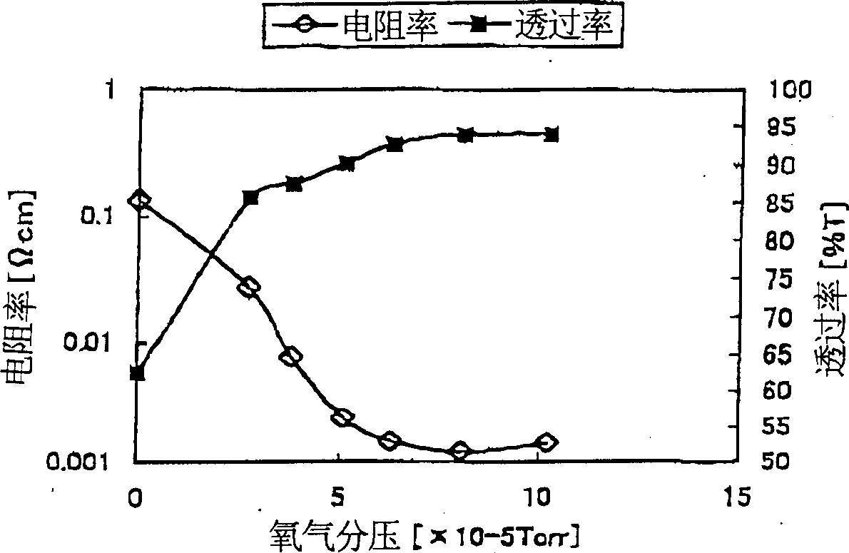
[0047] Prepare In with a purity >99.99% 2 o 3 Powder and SnO 2 Powder, and SiO with purity>99.9% 2 pink. According to SnO 2 10wt%, SiO 2 5wt%, In 2 o 3 This powder was prepared at a ratio of 85% by weight and a total amount of 1.5 Kg (Si corresponds to about 0.13 mol to 1 mol of In), and a molded body was obtained by filtration molding. Then, the sintered body was fired and sintered in an oxygen atmosphere at 1550° C. for 8 hours. This sintered body was processed to obtain a target having a relative density of 100% to the theoretical density. The volume resistivity of the target is 2.4×10 -4 Ωcm.

[0048] Using this target, a film was formed by DC magnetron sputtering under the following conditions to obtain a film with a thickness of 1200 Å.

[0049] Target size: φ=6in.τ=6mm

[0050] Sputtering method: DC magnetron sputtering

[0051] Exhaust device: rotary pump + cryopump

[0052] Reached vacuum degree: 4.0×10 -5 [Torr]

[0053] Ar pressure: 3.0×10 -3 [Torr]...

Embodiment 2

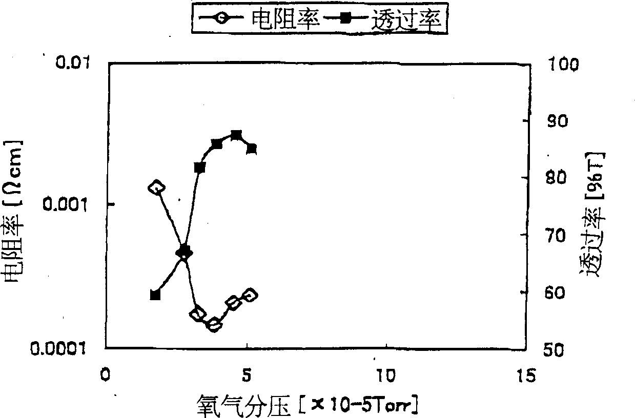
[0063] Prepare In with a purity >99.99% 2 o 3 Powder and SnO 2 Powder, and SiO with purity>99.9% 2 pink. According to SnO 2 10wt%, SiO 2 10wt%, In 2 o 3 This powder was prepared at a ratio of 80 wt % and a total amount of 1.5 Kg (Si corresponds to about 0.26 mol to 1 mol of In), and a molded body was obtained by filtration molding. Then, the sintered body was fired and sintered in an oxygen atmosphere at 1550° C. for 8 hours. This sintered body was processed to obtain a target having a relative density of 100% to the theoretical density. The volume resistivity of the target is 4.0×10 -4 Ωcm.

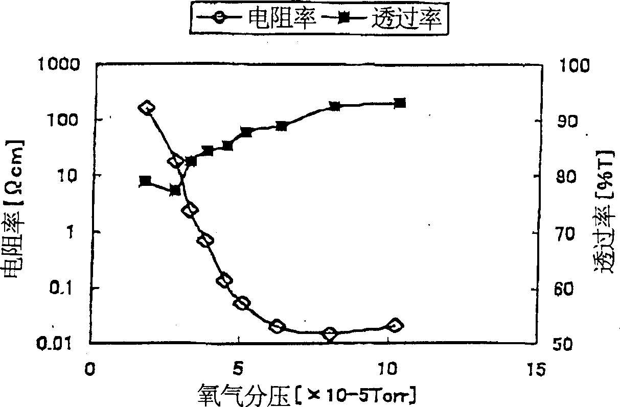
[0064] Using this target, a film was formed by DC magnetron sputtering under the same conditions as in Example 1 to obtain a film with a thickness of 1200 Å. By analyzing the resistivity and transmittance of the film, we get image 3 Such a relationship between the resistivity against the partial pressure of oxygen and the transmittance at a wavelength of 550 nm.

Embodiment 3

[0066] Prepare In with a purity >99.99% 2 o 3 Powder and SnO 2 Powder, and SiO with purity>99.9% 2 pink. According to SnO 2 10wt%, SiO 2 5wt%, In 2 o 3 This powder was prepared at a ratio of 85% by weight and a total amount of 1.5 Kg (Si corresponds to about 0.13 mol to 1 mol of In), and a molded body was obtained by filtration molding. Then, the fired body was fired and sintered in an oxygen atmosphere at 1450° C. for 8 hours. This sintered body was processed to obtain a target having a relative density of 100% to the theoretical density. The volume resistivity of the target is 3.0×10 -4 Ωcm.

[0067] Using this target, a film was formed by DC magnetron sputtering under the same conditions as in Example 1 to obtain a film with a thickness of 1200 Å. Analyzing the resistivity and transmittance of the film, it was shown that the same figure 1 Nearly equivalent oxygen partial pressure characteristics.

[0068] As can be seen from the above results, the volume resist...


PUM

PropertyMeasurementUnit
electrical resistanceaaaaaaaaaa

Abstract

PROBLEM TO BE SOLVED: To provide a sputtering target for a highly resistant transparent conductive film which can be basically used in a DC magnetron sputtering apparatus, and can deposit a transparent and highly resistant film, and to provide a method of manufacturing the highly resistant transparent conductive film.SOLUTION: The indium oxide sputtering gate for the highly resistant transparent conductive film to deposit the highly resistant transparent conductive film with the resistivity of about 0.8-10×10<SP>-3< / SP>&Omega;-cm contains indium oxide and tin oxide as necessary, and also contains an insulating oxide.

Description

technical field [0001] The present invention relates to making resistivity about 0.8~10×10 -3 A high-resistance transparent conductive film sputtering target (Sputtering target) used for a high-resistance conductive film of Ωcm and a method for producing a high-resistance transparent conductive film using the sputtering target. Background technique [0002] Since indium oxide-tin oxide (In 2 o 3 -SnO 2 composite oxide, hereinafter referred to as 'ITO') film has high visible light transmittance and high conductivity, so it is widely used as a transparent conductive film for liquid crystal display devices, heat-generating films for preventing frosting on glass, and infrared reflective films Wait. [0003] For example, for a transparent conductive film used in a flat panel display (FPD), low resistance (resistivity of about 2×10 -4 Ωcm) transparent conductive film. [0004] On the other hand, in principle, a transparent conductive film for a resistive key pad used for mou...

Claims


Application Information

Patent Timeline
Patent Type & Authority Applications(China)
IPC IPC(8): C04B35/00C23C14/08C23C14/34
CPCA22C29/021A22C29/043A23L17/40B08B3/02
Inventor 高桥诚一郎池田真渡边弘
Owner MITSUI MINING & SMELTING CO LTD
Learn More