Semiconductor device

A semiconductor, conduction technology, applied in the direction of semiconductor devices, output power conversion devices, transistors, etc., can solve problems such as deviation, short circuit of power devices 12 and 13, etc.

Inactive Publication Date: 2003-02-26
MITSUBISHI ELECTRIC CORP
View PDF1 Cites 16 Cited by
  • Summary
  • Abstract
  • Description
  • Claims
  • Application Information

AI Technical Summary

Problems solved by technology

[0024] However, although the protection circuit 8 functions as a filter when the false pulses caused by the dv / dt transition signal are simultaneously supplied as the signals S2 and S3, when the false pulses P1 and P2 caused by the dv / dt transition signal are caused by the HNMOS transistor 4 and When there is a time difference supply due to the deviation of the element characteristics of 5, in the output signals S6 and S7 of the protection circuit 8, pulse signals P11 and P12 with a width corresponding to the time difference are supplied, so that the power device 12 will be caused by the pulse signals P11 and P12. Misoperation in on-state or off-state
[0025] Moreover, when the power device 12 malfunctions, it will maintain the malfunction until the next normal ON signal or OFF signal is supplied. Depending on the situation, the power devices 12 and 13 may be short-circuited or the like.

Method used


Image

  • Semiconductor device
  • Semiconductor device
  • Semiconductor device

Examples


Embodiment 1

[0088] A-1. Device structure

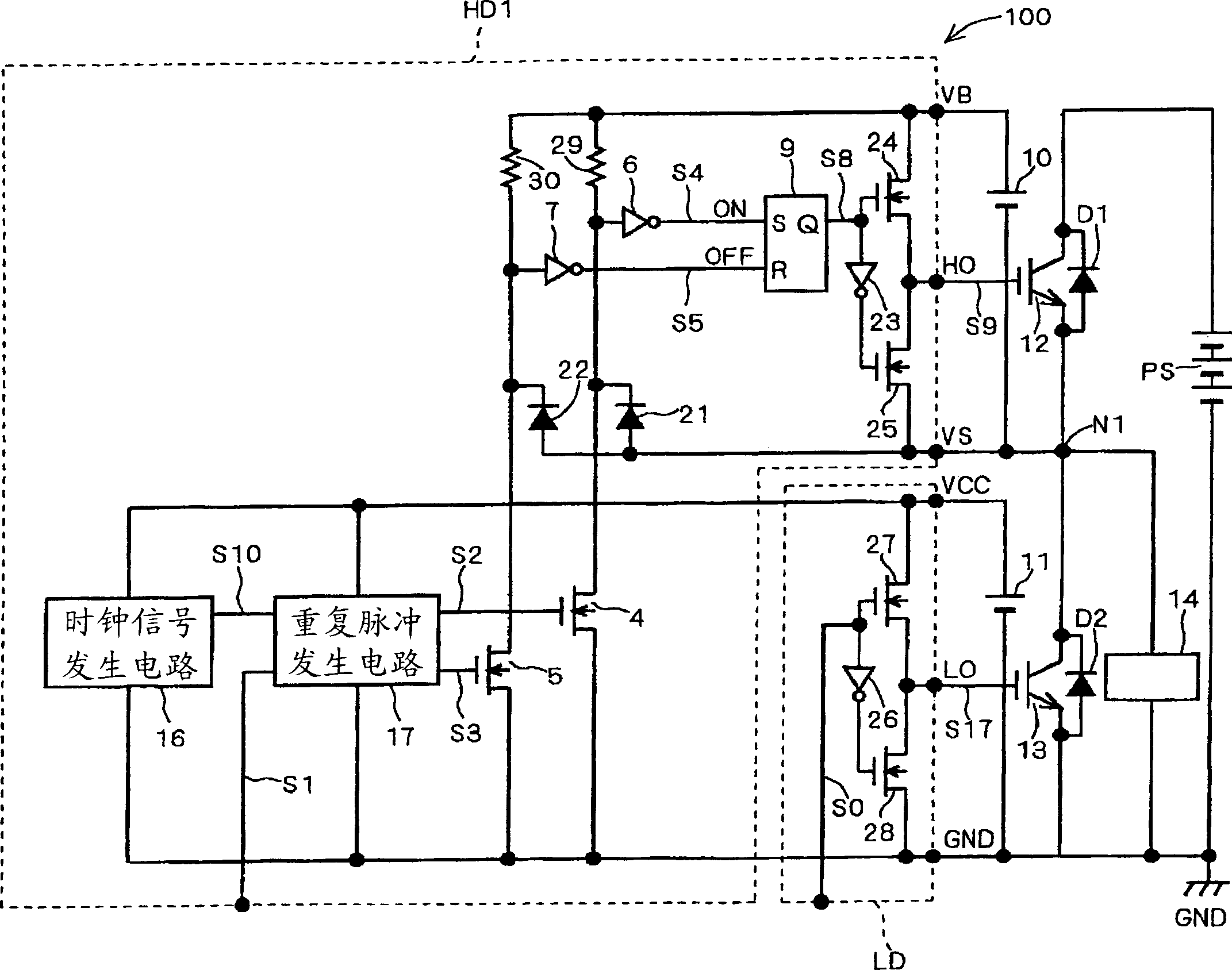
[0089] As Embodiment 1 of the semiconductor device of the present invention, figure 1 The structure of the level shift circuit 100 in the state mode is shown.

[0090] exist figure 1 Among them, the power devices 12 and 13 such as IGBT (insulated gate bipolar transistor) are connected between the positive pole and the negative pole (ground potential GND) of the power supply PS in a push-pull type to form a half-bridge power device. In addition, freewheeling diodes D1 and D2 are connected in parallel with power devices 12 and 13 in reverse direction, respectively. Furthermore, a load (inductive load such as a motor) 14 is connected to a connection point N1 between the power device 12 and the power device 13 .

[0091] exist figure 1 Among them, the power device 12 uses the potential of the connection point N1 with the power device 13 as a reference potential, and switches between the reference potential and the power supply potential suppli...

Embodiment 2

[0123] B-1. Device structure

[0124] As Embodiment 2 of the semiconductor device of the present invention, Figure 4 The structure of the level shift circuit 200 is shown. exist Figure 4 in, for with figure 1 The same structures of the level shift circuit 100 shown are denoted by the same symbols, and repeated explanations are omitted.

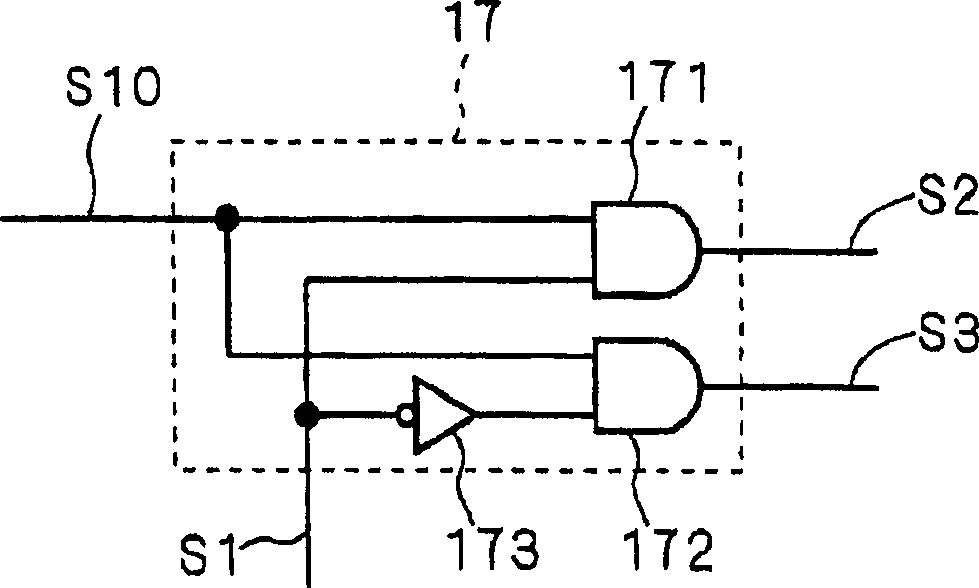
[0125] Such as Figure 4 As shown, the level shift circuit 200 is divided into a high potential side power device drive circuit HD2 and a low potential side power device drive circuit LD. In the high potential side power device drive circuit HD2, there is no figure 1 The clock signal generation circuit 16 provided in the shown level shift circuit 100 supplies a clock signal supplied from the outside as a signal S10 to the repetitive pulse generation circuit 17 .

[0126] exist figure 1 In the shown level shift circuit 100, the pulse signal generated by the own clock signal generation circuit 16 is used. However, at this time, the ti...

Embodiment 3

[0137] C-1. Device structure

[0138] As Embodiment 3 of the semiconductor device of the present invention, Figure 6 The configuration of the level shift circuit 300 is shown. exist Figure 6 in, for and figure 1 The same structures of the level shift circuit 100 shown are denoted by the same symbols, and repeated explanations are omitted.

[0139] Such as Figure 6 As shown, the level shift circuit 300 is divided into a high potential side power device drive circuit HD3 and a low potential side power device drive circuit LD. In the high potential side power device drive circuit HD3, there is a level shifted OR circuit 19 that obtains a clock signal with the same frequency as the oscillation frequency of clock signal generating circuit 16 in the high potential area by logical sum of on-signal S4 of one bit and off-signal S5 that has been level-shifted.

[0140] That is, the outputs of the inverter circuits 6 and 7 are connected to the set input and reset input of the SR...


PUM


Abstract

Provided is a level shifting circuit capable of preventing a power device from a malfunction also when a dv/dt transient signal is supplied with time difference. A high-potential side power device driving circuit has a clock signal generation circuit generating the so-called internal clock signal by outputting a pulse in a constant cycle for driving NMOS transistors and an iterative pulse generation circuit monitoring the state of an external input signal in synchronization with an output signal of the clock signal generation circuit, receiving a pulsing input signal generated with reference to a ground potential and generating pulsing ON and OFF signals.

Description

technical field [0001] The present invention relates to a semiconductor device, especially a level shift circuit of a power device for preventing malfunction caused by a dv / dt transition signal. Background technique [0002] Figure 36 The structure of the level shift circuit 90 of a conventional power device is shown. Figure 36 The structure shown is disclosed in JP-A-9-200017. [0003] exist Figure 36 Among them, the power devices 12 and 13 such as IGBT (insulated bipolar transistor) are push-pull connected between the positive pole and the negative pole (ground potential GND) of the power supply PS to form a half-bridge power device. In addition, freewheeling diodes D1 and D2 are connected in parallel with power devices 12 and 13 in reverse direction, respectively. Furthermore, a load (inductive load such as a motor) 14 is connected to a connection point N1 between the power device 12 and the power device 13 . [0004] exist Figure 36 Among them, the power device 12 ...

Claims


Application Information

Patent Timeline
Patent Type & Authority Applications(China)
IPC IPC(8): H02M1/08H03K17/06H03K17/08H03K17/0812H03K17/10H03K17/16H03K17/56H03K19/0175
CPCH03K17/08128H03K17/107H03K17/063H03K17/16
Inventor 冈本和明荒木达
Owner MITSUBISHI ELECTRIC CORP
Why Eureka
Try Eureka