Lithium niobate modulator and its making process

A manufacturing method and technology of lithium niobate, applied in instruments, electromagnetic wave transmission systems, optics, etc., can solve problems such as large insertion loss, high half-wave voltage, and low extinction ratio

Inactive Publication Date: 2003-05-14
HUAWEI TECH CO LTD
View PDF0 Cites 44 Cited by
  • Summary
  • Abstract
  • Description
  • Claims
  • Application Information

AI Technical Summary

Problems solved by technology

M-Z type device or higher rate lithium niobate M-Z type modulator, even the 2.5Gb/s lithium niobate modulator sample c

Method used


Image

  • Lithium niobate modulator and its making process
  • Lithium niobate modulator and its making process
  • Lithium niobate modulator and its making process

Examples


Embodiment Construction

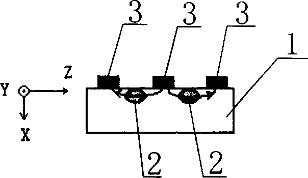
[0034] Such as Figure 1 to Figure 14 As shown, the lithium niobate modulator of the present invention includes:

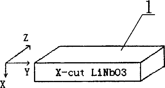
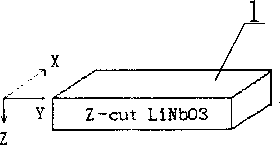
[0035] The substrate 1 is prepared from a lithium niobate crystal with a suitable crystal tangential direction and electric field utilization direction; the electro-optical coefficients of the lithium niobate crystal in each direction are not the same. In order to obtain the maximum modulation efficiency in this embodiment, the modulation electrode is designed When using the maximum electro-optic coefficient γ of lithium niobate crystal 33 , that is, the electric field direction is parallel to the Z-axis direction of the crystal. When making lithium niobate optical waveguides, you can choose X-cut crystals or Z-cut crystals. The difference between the two is that the insertion loss of optical waveguides based on X-cut crystals is relatively small, while that based on Z-cut crystals The waveguide light effect is better than the former. gamma 33 The utilization ...


PUM

PropertyMeasurementUnit
Thicknessaaaaaaaaaa
Thicknessaaaaaaaaaa
Thicknessaaaaaaaaaa

Abstract

The making process of lithium niobate modulator includes making substrate with lithium niobate crystal with proper crystal cutting direction and electric field utilizing direction; making light waveguide on the lithium niobate crystal; making modulating electrodes including central signal electrode and earth electrode and to form push-pull structure with the light waveguide; making microstrip matching structure in the input and output of the modulating electrodes; and setting buffering layer structure between the modulating electrode and light waveguide. Owing to the smart design of the modulating electrodes, the light waveguide and the matching structure in between, the lithium niobate modulator has high modulating rate, low insertion loss, high extinction ratio, low hemi-wave voltage, less electric reflection, and high reliability.

Description

technical field [0001] The invention relates to a lithium niobate LiNbO 3 The modulator and its manufacturing method belong to the improvement of high-speed optical communication devices. Background technique [0002] Modulation can be divided into two types, one is direct modulation, which is realized by directly changing the injection current of the laser. This method is simple, economical and easy to implement, but it is difficult to overcome its own frequency drift during high-speed modulation, so it can only be used for Dispersion-insensitive low-speed communication systems, such as STM-1 / STM-4. The second is indirect modulation, also known as external modulation. It is realized by letting the beam emitted by the laser pass through an external modulator that can change the amplitude or phase of the beam. There are three main types of external optical modulators commonly used at present: monolithic integration (III- V) Active M-Z modulator, electron absorption (EA) ext...

Claims


Application Information

Patent Timeline
IPC IPC(8): G02F1/03H04B10/25
Inventor 蒲天春谭松李汉国曹宏斌蔡义智
Owner HUAWEI TECH CO LTD
Why Eureka
Try Eureka