Silicon-based high-speed dual-carrier double-polarization modulator integrated chip

A technology of integrated chips and modulators, applied in the field of silicon-based high-speed dual-carrier dual-polarization modulator integrated chips, can solve the problems of high power consumption and large volume of optical modulators, and achieve low power consumption, small volume, and guaranteed yield Effect

Active Publication Date: 2017-05-31
INST OF SEMICONDUCTORS - CHINESE ACAD OF SCI
View PDF9 Cites 9 Cited by
  • Summary
  • Abstract
  • Description
  • Claims
  • Application Information

AI Technical Summary

Problems solved by technology

[0005] Since the communication rate and capacity of the traditional dense wavelength division multiplexing optical communication system can no longer meet people's growing information needs, and the traditional optical modulator is large in size and high in power consumption, the big data forwarding of the communication center base station is facing a bottleneck. Therefore, At present, there is an urgent need for high-order modulation code modulation, stability, low power consumption, and small-volume optical modulators to solve these problems

Method used


Image

  • Silicon-based high-speed dual-carrier double-polarization modulator integrated chip
  • Silicon-based high-speed dual-carrier double-polarization modulator integrated chip
  • Silicon-based high-speed dual-carrier double-polarization modulator integrated chip

Examples


Embodiment Construction

[0039] In order to make the object, technical solution and advantages of the present invention clearer, the present invention will be further described in detail below in conjunction with specific embodiments and with reference to the accompanying drawings.

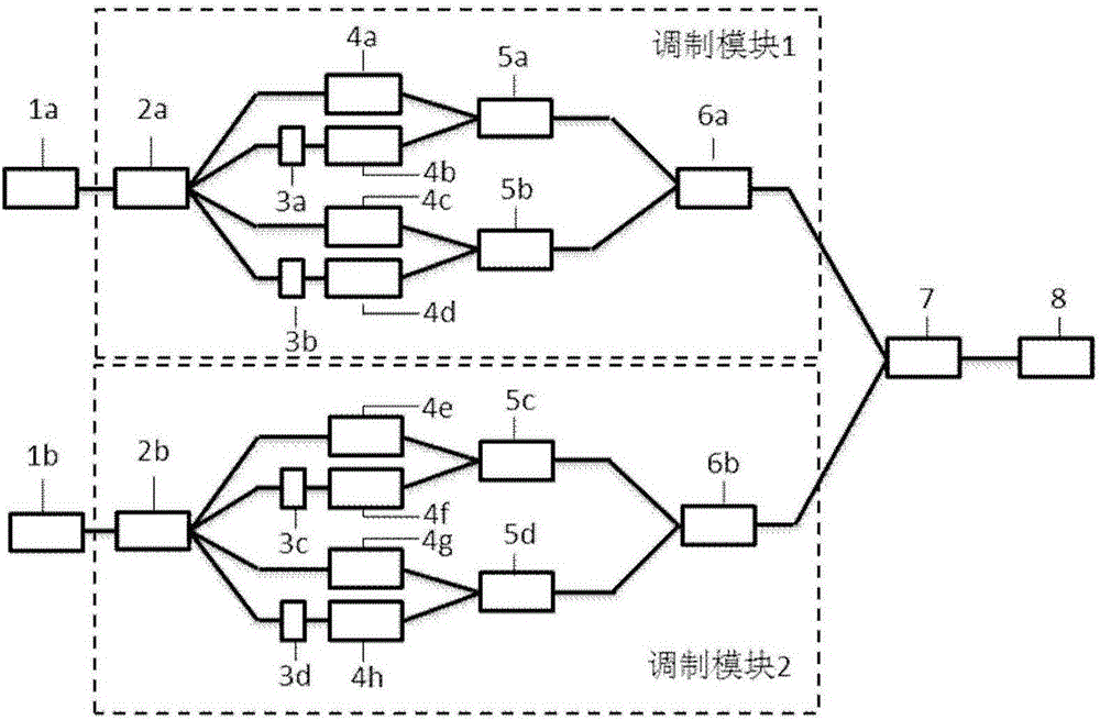
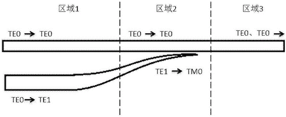
[0040] The invention provides a silicon-based high-speed dual-carrier dual-polarization modulator integrated chip, which includes 2 single-mode vertical coupling gratings, 2 modulation modules, 1 2×1 multi-mode interference coupler, and 1 dual-mode vertical coupling grating . Silicon-based transverse electric mode (TE0) waveguide connection is used between the two single-mode vertical coupling gratings and the two modulation modules, wherein the transverse electric mode is transmitted; between the modulation module and the 2×1 multimode interference coupler, and The 2×1 multimode interference coupler and the dual-mode vertical coupling grating are connected through a multimode waveguide, in which the transverse electric m...


PUM


Abstract

The invention discloses a silicon-based high-speed dual-carrier double-polarization modulator integrated chip. The integrated chip comprises two single-mode vertical coupling gratings, two modulation modules, one 2 * 1 multimode interference coupler and one dual-mode vertical coupling grating. The silicon-based high-speed dual-carrier double-polarization modulator integrated chip can work in a dual-wavelength double-polarization state, and can combine polarization multiplexing with wavelength division multiplexing to achieve complex format modulation and improve the data modulation rate. The silicon-based high-speed dual-carrier double-polarization modulator integrated chip can realize double-polarization hexadecimal quadrature amplitude modulation so as to satisfy the high-order format modulation required by the next generation optical communication system, and the modulation rate can reach and even exceed 400 Gbit / s.

Description

technical field [0001] The invention relates to a high-speed electro-optical modulator used in a high-speed optical communication system, in particular to a silicon-based high-speed dual-carrier dual-polarization modulator integrated chip. Background technique [0002] Since the 21st century, people's demand for information has exploded like never before. The development of optical fiber communication technology has led to the construction of high-speed, large-capacity communication networks. China also proposed the "Broadband China" national strategy in 2013, incorporating the construction of high-speed and large-capacity networks into the national development plan. However, at present, countries around the world have successively laid relatively complete existing optical fiber communication networks based on dense wavelength division multiplexing technology. Facing the ever-increasing demand for information, the capacity of traditional dense wavelength division multiplexi...

Claims


Application Information

Patent Timeline
Patent Type & Authority Applications(China)
IPC IPC(8): H04B10/516H04B10/54
CPCH04B10/516H04B10/5161H04B10/541G02F1/025G02F1/2257G02F2201/06G02F2201/18G02F2201/302G02F2203/07G02F1/212
Inventor 李明唐健刘宇袁海庆祝宁华
Owner INST OF SEMICONDUCTORS - CHINESE ACAD OF SCI
Why Eureka
Try Eureka