

Semiconductor IC and mfg. method thereof
An integrated circuit and semiconductor technology, applied in the field of semiconductor integrated circuits, can solve problems such as increasing the test time, and achieve the effect of shortening the test time and preventing the increase of the chip size
- Summary
- Abstract
- Description
- Claims
- Application Information
AI Technical Summary
Problems solved by technology
Method used
Image

Examples
Embodiment Construction
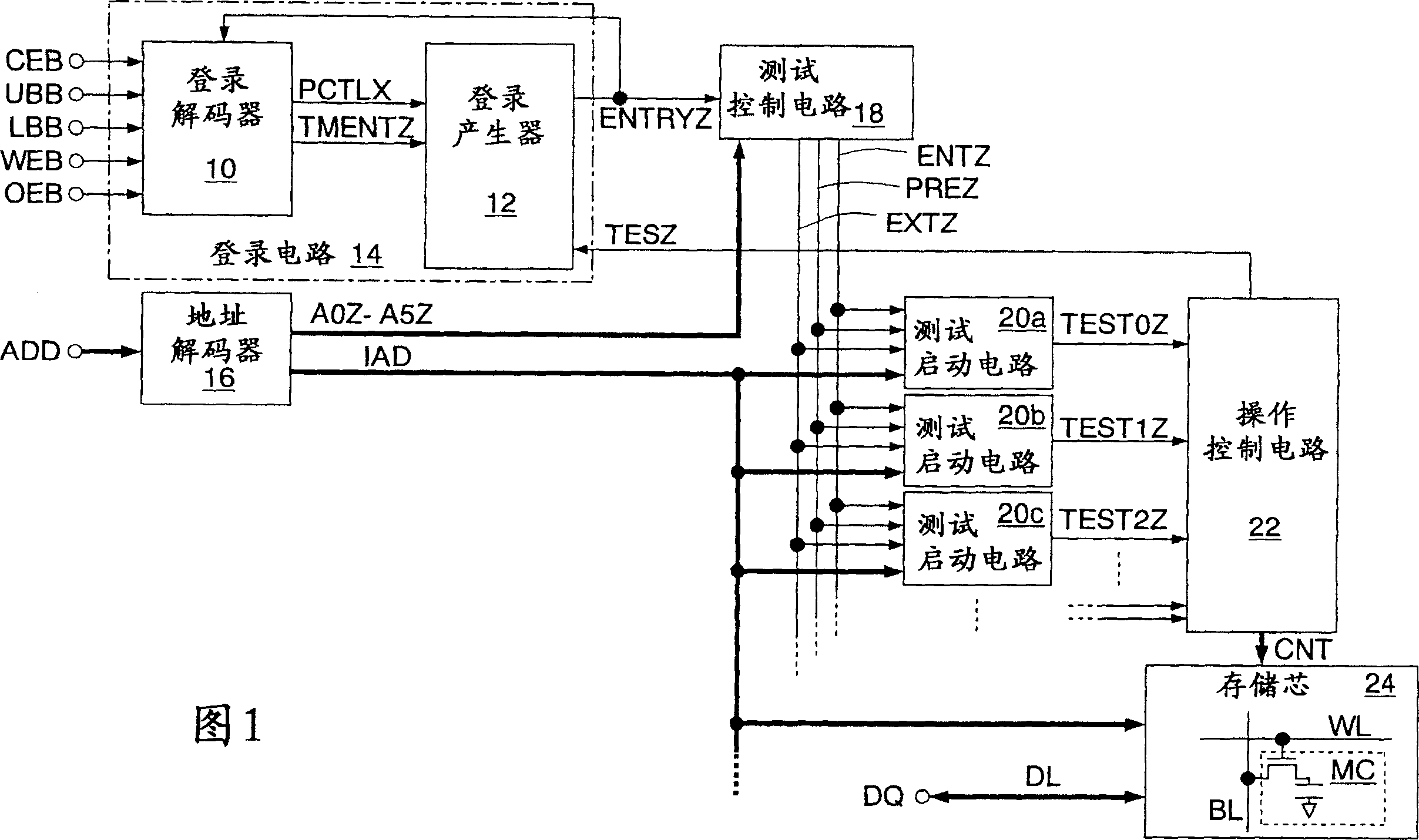
[0023] Hereinafter, preferred embodiments of the present invention will be described with reference to the accompanying drawings. In the figure, each signal line shown by a thick line includes a plurality of lines. Signals with a "Z" as the last letter indicate positive logic, and signals with a "B" or "X" as the last letter indicate negative logic.
[0024] FIG. 1 shows an embodiment of the semiconductor integrated circuit of the present invention. The semiconductor integrated circuit is formed on a silicon substrate by using CMOS processing as a clock asynchronous DRAM. The DRAM has a login circuit 14 including a login decoder 10 and a record generator 12, an address decoder 16, a test control circuit 18, a plurality of test start circuits 20 (20a, 20b, 20c, . . . ), an operation control circuit 22. and memory core 24 . In this figure, dots at the ends of the signal lines represent external terminals.
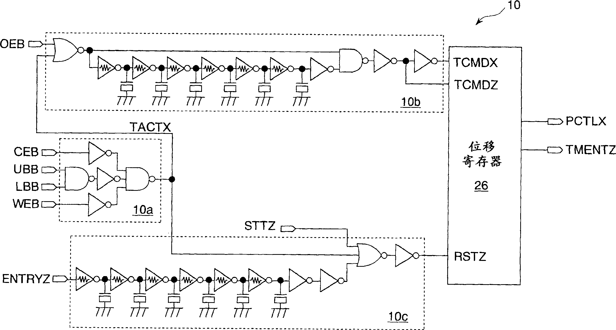
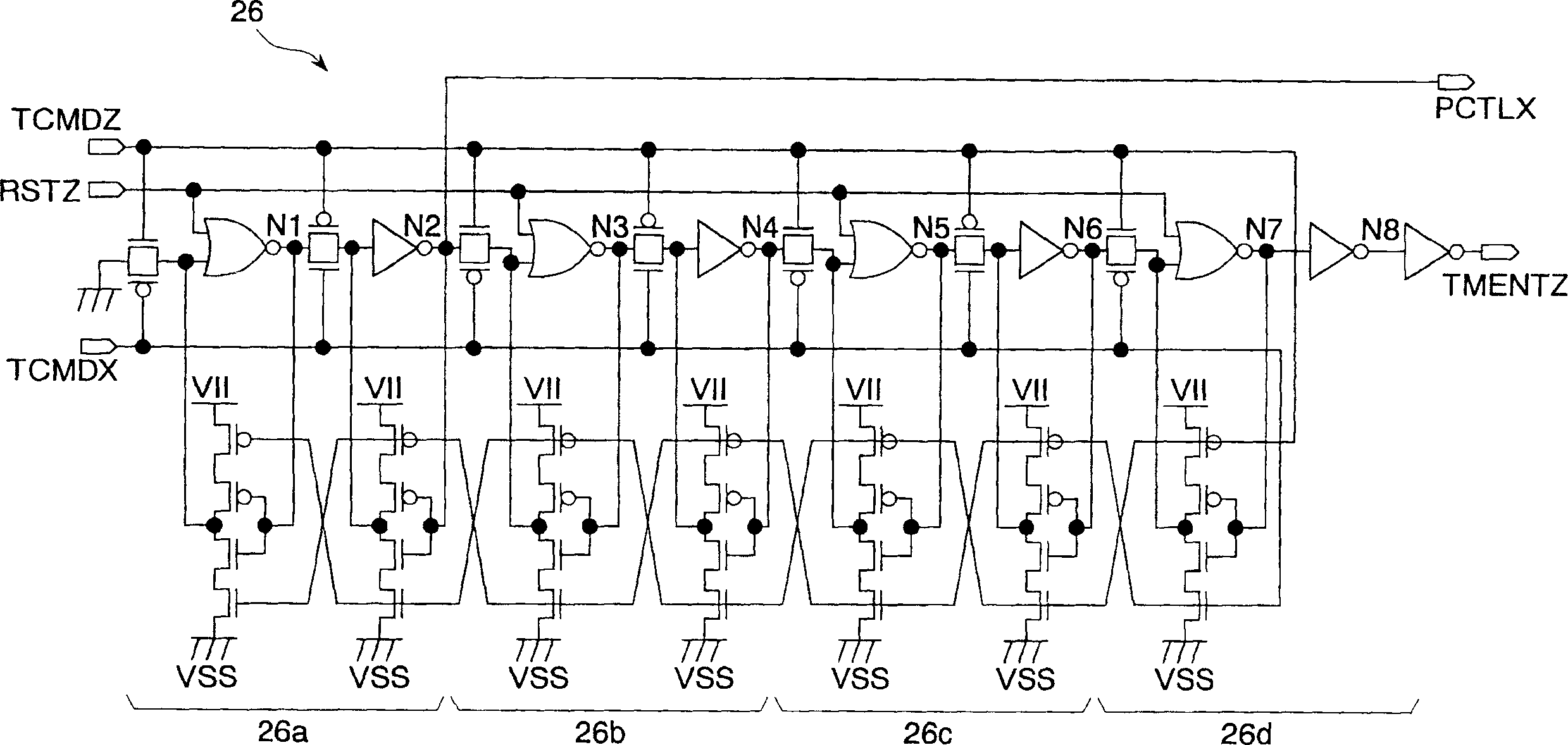
[0025] Login decoder 10 receives control command CMD (chip enable si...
PUM
 Abstract
Description
Claims
Application Information