Welding method and welding device

A welding method and welding device technology, applied in welding equipment, non-electric welding equipment, electrical components, etc., can solve problems such as uneven size, cut leads, and inability to guarantee welding quality, and achieve constant quality and reliability. Effect

Inactive Publication Date: 2003-07-16
SEIKO EPSON CORP
View PDF0 Cites 2 Cited by
  • Summary
  • Abstract
  • Description
  • Claims
  • Application Information

AI Technical Summary

Problems solved by technology

[0004] However, according to this process, during the rising process, the capillary and the lead wire rub against each other, and the lead wire may be cut off before reaching a given length.
Like this, for each welding process, the distance between the welding torch and the front end

Method used


Image

  • Welding method and welding device
  • Welding method and welding device
  • Welding method and welding device

Examples


Example

[0053] (first embodiment)

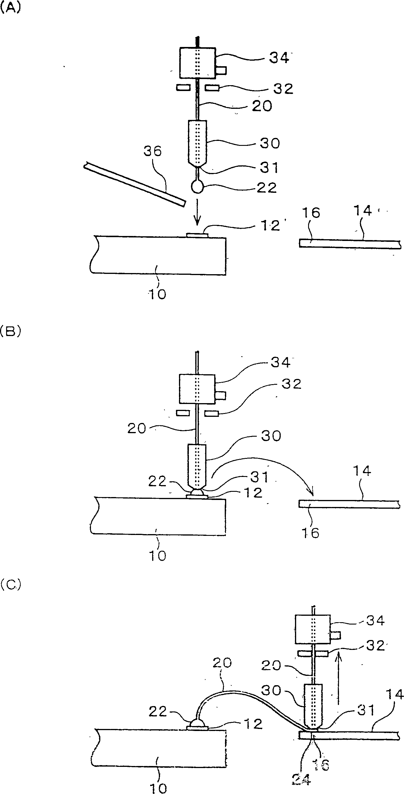
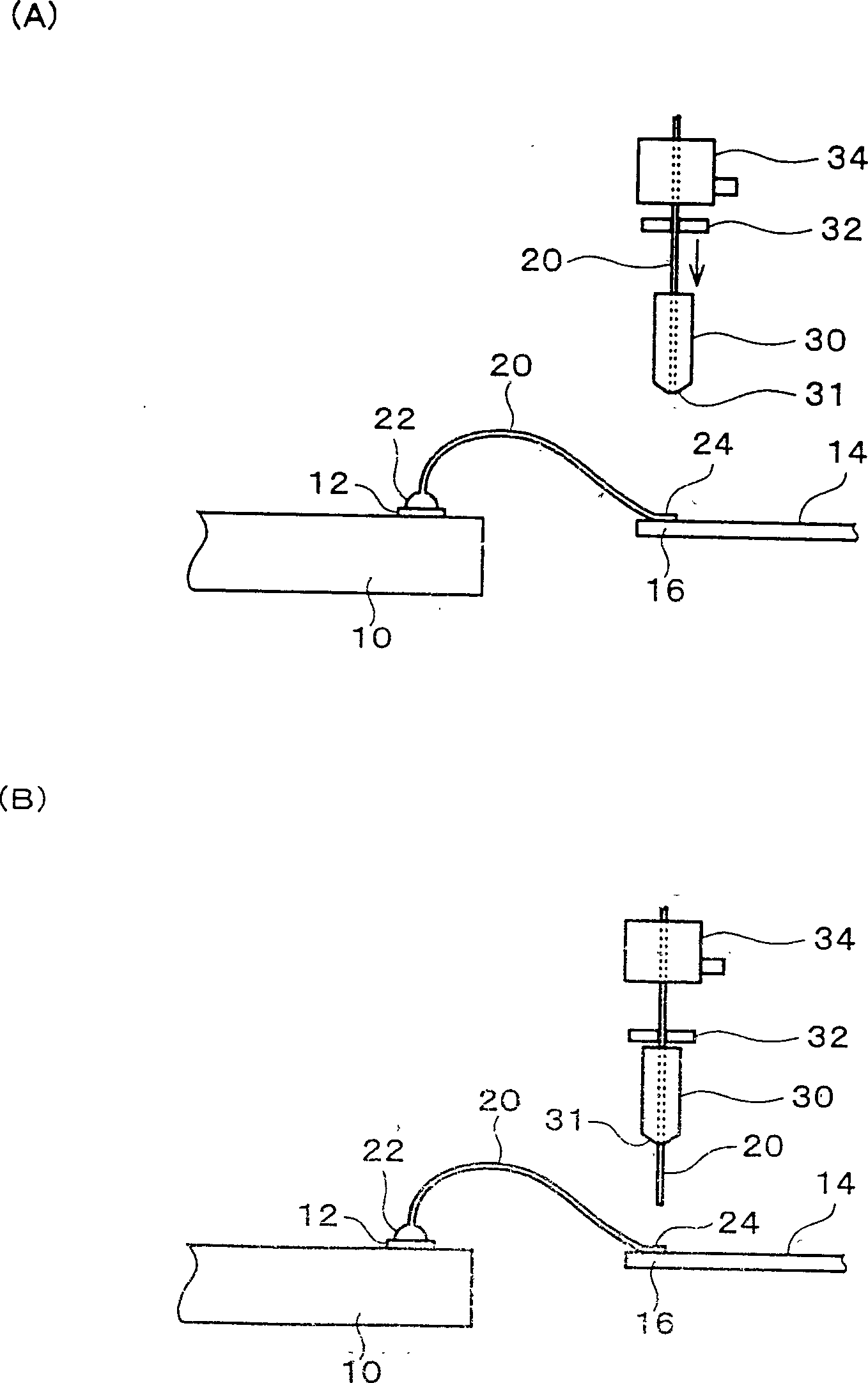
[0054] figure 1 A~ figure 2 B is a diagram showing a semiconductor device manufacturing method and manufacturing apparatus (also referred to as a wire bonding method and a wire bonding apparatus) according to the first embodiment of the present invention.

[0055] First, if figure 1 As shown in A, a semiconductor chip 10 on which a plurality of pads 12 and a plurality of leads 14 are formed is prepared.

[0056]The semiconductor chip 10 has a surface (active surface) on which an integrated circuit is formed. The integrated circuit is formed on the surface of the largest area of ​​the semiconductor chip 10 which is a rectangular parallelepiped. The pads 12 are often formed on the side of the surface of the semiconductor chip 10 on which the integrated circuit is formed. The pads 12 are formed of aluminum-based or copper-based metals, and are often formed as a flat thin layer on the semiconductor chip 10 . Also, on the semiconductor chip 10, a ...

Example

[0082] (second embodiment)

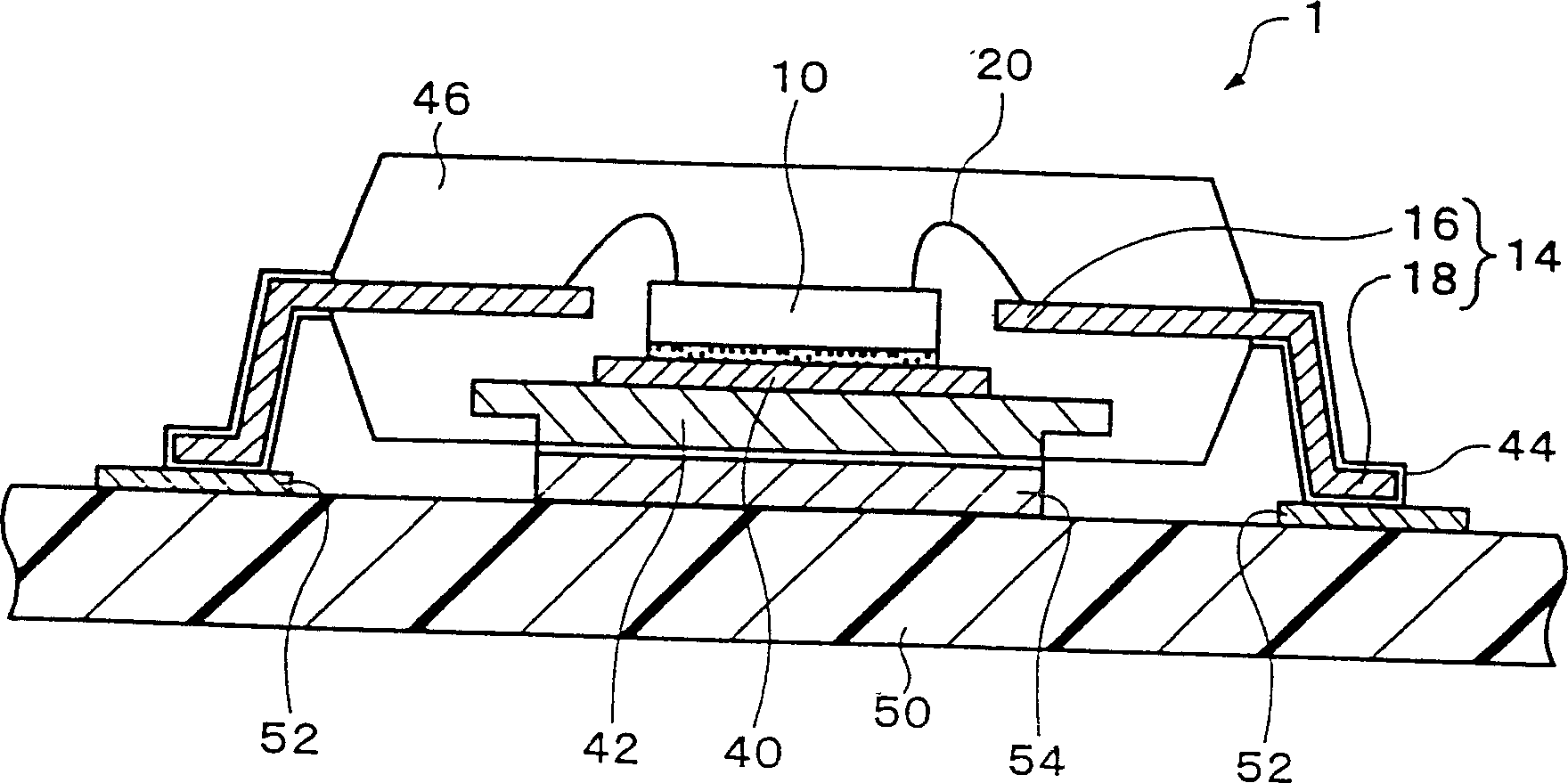
[0083] Figure 4 A~ Figure 5 B is a diagram showing a semiconductor device manufacturing method and manufacturing apparatus (also referred to as a bump forming method and a bump forming apparatus) according to the second embodiment of the present invention. In this embodiment mode, the semiconductor device manufacturing apparatus described in the above-mentioned embodiment mode can be used. In addition, in this embodiment, any one of the contents described in the above embodiments can be selectively applied.

[0084] First, if figure 1 As shown in A, a semiconductor wafer 60 is prepared. The semiconductor wafer 60 includes a surface (active surface) on which integrated circuits are formed. Then, a plurality of pads 62 are formed on the side of the semiconductor wafer 60 on which the integrated circuits are formed. In addition, a passivation film (not shown) may be formed on the semiconductor wafer 60 other than the pads 62 . In the present ...


PUM


Abstract

A tip of a wire is formed in a shape of a ball, the wire being inserted into and fed out of a first tool. The tip is bonded to a first electrode by using the first tool. The wire is drawn from the first tool and a part of the wire is bonded to a second electrode by using the first tool. The wire is held by a second tool disposed above the first tool, and cut in a state to allow the part of the wire to remain on the second electrode. The wire is fed out of the first tool by positioning the first and second tools relatively closer to each other while holding the wire by the second tool.

Description

technical field [0001] The invention relates to a welding method and a welding device. Background technique [0002] In the manufacture of semiconductor devices, a wire bonding process for electrically connecting pads and leads of a semiconductor chip is performed. In this process, the tip of the lead drawn from the capillary to the outside is formed into a ball by a torch, the ball is soldered to the pad, and the lead is drawn out and soldered to the pin. [0003] Then, a lead wire of a given length is drawn out from the capillary, and then the lead wire is cut. Specifically, with the lead wire connected to the pin, the jig holding the lead wire is released, the jig and the capillary are raised at the same time, the lead wire of a given length is drawn out from the capillary tube, and then the lead wire is cut. [0004] However, according to this process, the capillary and the lead wire rub against each other during the ascent, and the lead wire may be cut off before reac...

Claims


Application Information

Patent Timeline
IPC IPC(8): H01L21/60B23K20/00B23K31/00H01L21/00H01L21/44H01L21/607
CPCH01L2224/73265H01L2224/48235H01L24/45H01L2224/05647H01L2224/32225H01L2224/85181H01L2224/48624H01L2924/0105H01L2224/48091H01L2924/00013H01L2224/16225H01L2924/01004H01L2924/01078H01L2924/01006H01L2924/01079H01L2924/14H01L2224/85205H01L2224/32245H01L2924/15311H01L2224/16B23K20/005H01L2924/01005H01L24/78H01L2924/01082H01L2224/73204H01L2224/13099H01L2924/01013H01L2224/45144H01L2224/85045H01L2224/1134H01L24/85H01L2924/014H01L2224/0401H01L2924/01029H01L2224/48247H01L2224/05624H01L2224/48647H01L2224/48465H01L2224/78301H01L2924/01033H01L2224/45015H01L2924/181H01L24/48H01L2924/00014H01L2924/00H01L2924/00012
Inventor 三上邦光
Owner SEIKO EPSON CORP
Why Eureka
Try Eureka