Thick oxide layer on botton of trench structure in silicon

A technology of oxide layer and dioxide layer, which is applied in the direction of semiconductor devices, electrical components, transistors, etc., and can solve problems such as reduced efficiency

Inactive Publication Date: 2003-10-08
FAIRCHILD SEMICON CORP
View PDF0 Cites 10 Cited by
  • Summary
  • Abstract
  • Description
  • Claims
  • Application Information

AI Technical Summary

Problems solved by technology

However, a thicker uniform gate dielectric layer requires a higher gate charge, which reduces efficiency

Method used


Image

  • Thick oxide layer on botton of trench structure in silicon
  • Thick oxide layer on botton of trench structure in silicon
  • Thick oxide layer on botton of trench structure in silicon

Examples


Embodiment Construction

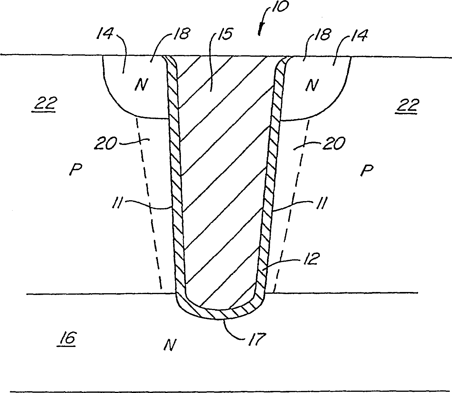
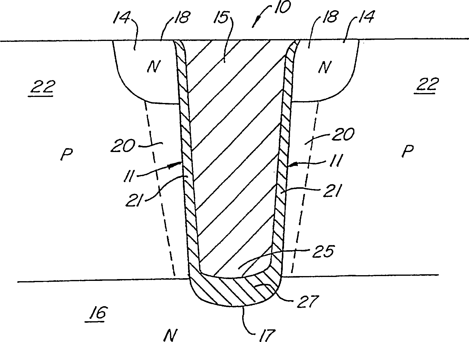
[0016] figure 2 is an exemplary N-channel transistor with an excellent gate insulation structure according to an embodiment of the present invention. The trench 10 with sidewalls 11 and bottom 17 extends into a silicon substrate body region 22 . figure 2 The sources shown are represented by two N-type regions 14 adjacent and opposite the channel 10 . The drain is represented by an N-type region below the P-type body region 22 . It will be appreciated that in the case of p-type transistors, the conductivity types of the respective drain, source and body regions may be reversed. The conductive material forms the gate 15 of the channel transistor. The gate 15 may extend above, below or at the same level as the surface of the main body region 22 of the silicon substrate. In operation, the drain region 16 may be electrically contacted by the substrate of the device, the gate may be electrically contacted by a conductive layer (e.g., aluminum) above a transistor, and the active ...


PUM


Abstract

A gate isolation structure of a semiconductor device and method of making the same provides a trench in a silicon substrate, wherein a dielectric layer is formed on sidewalls and bottom of the trench, the dielectric layer having a first thickness on the sidewalls and a second thickness at the bottom that is greater than the first thickness. The thicker dielectric layer at the bottom substantially reduces gate charge to reduce the Miller Capacitance effect, thereby increasing the efficiency of the semiconductor device and prolonging its life.

Description

[0001] References to related applications [0002] The first related patent application is Attorney Docket No. 0168865-003300US, in the name of Izak Bencuya et al., filed concurrently with this application, and entitled "Vertical MOSFET with Ultra-LowResistance and Low Gate Charge," which has been assigned to the present assignee. A second related patent application is U.S. Patent Application No. ___, entitled "Selective Oxide Deposition in the Bottom of a Trench," in the name of James J. Murphy, Attorney Docket No. 0168865-004800US, filed concurrently with this application , which has been assigned to the present assignee. Both applications are hereby incorporated by reference. (1) Technical field [0003] The present invention relates generally to field effect transistors, and more particularly to channel transistors and methods of manufacturing the same. (2) Background technology [0004] FIG. 1 is a simplified cross-section of a portion of a conventional channel power...

Claims


Application Information

Patent Timeline
Patent Type & Authority Applications(China)
IPC IPC(8): H01L21/00H01L29/78H01L21/336H01L27/108H01L29/423H01L29/76H01L29/768H01L31/062
CPCH01L29/7827H01L29/66734H01L29/7813H01L29/42368H01L29/66666
Inventor H·W·赫斯特J·J·默非
Owner FAIRCHILD SEMICON CORP
Why Eureka
Try Eureka