Semiconductor manufacturing system and process control method thereof

A technology for manufacturing systems and semiconductors, applied in semiconductor/solid-state device manufacturing, program control design, memory systems, etc., can solve problems such as complexity, low production efficiency, and increased manufacturing costs

Inactive Publication Date: 2003-10-15
MACRONIX INT CO LTD
View PDF0 Cites 2 Cited by
  • Summary
  • Abstract
  • Description
  • Claims
  • Application Information

AI Technical Summary

Problems solved by technology

Since there are many and complicated semiconductor manufacturing processes in the manufacture of integrated circuits, the above-mentioned method

Method used


Image

  • Semiconductor manufacturing system and process control method thereof
  • Semiconductor manufacturing system and process control method thereof
  • Semiconductor manufacturing system and process control method thereof

Examples


Embodiment Construction

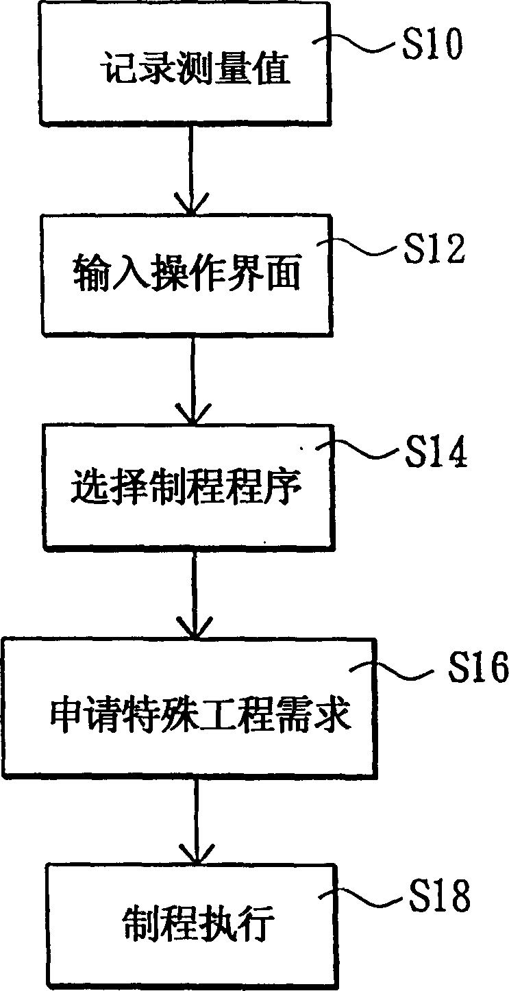
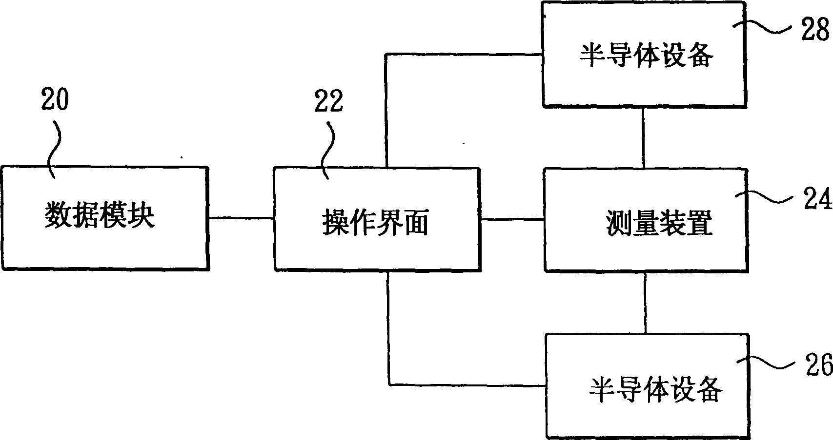
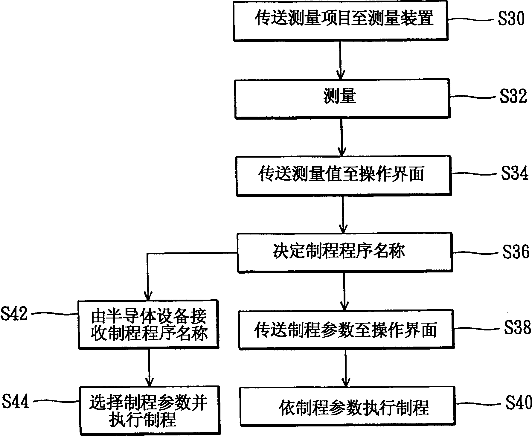
[0011] figure 2 with image 3 Respectively, a block diagram of a semiconductor manufacturing system according to an embodiment of the present invention and a flow chart of a control process program used therein.

[0012] First, in figure 2 In the illustrated embodiment, the semiconductor manufacturing system includes a data module (basic record, BR) 20 , an operation interface (operation interface, OPI) 22 , a measurement device 24 and semiconductor devices 26 and 28 . Wherein, the operation interface (OPI) 22 is associated with the data module (BR) 20, and both are included in a control system (not shown in the figure). The data module 20 has a measurement item field (not shown in the figure) and a process procedure identification field (not shown in the figure), the functions of which will be described later in this article.

[0013] In this embodiment, a measuring device 24, such as a thickness gauge, is coupled to the operation interface 22 of the control system. In ...


PUM


Abstract

The present invention relates to semiconductor manufacturing system and its program control process. The control of the manufacturing process includes: transmitting at least one measurement item viathe operation interface from the measurement item field of data module to the measuring installation and measuring to obtain corresponding measured value; storing via the operation interface one manufacture process condition table and determining the name of the manufacture process based on the measured value; transmitting manufacture process parameters corresponding to the manufacture process tothe operation interface via the manufacture process identifying field in data module based on the manufacture process name; accepting the manufacture process parameters via the self-operation interface in the semiconductor apparatus and executing the semiconductor manufacture process.

Description

technical field [0001] The invention relates to a semiconductor manufacturing system and a method for controlling its process program, in particular to a semiconductor manufacturing system and a method for controlling the process program that automatically determine the process program to execute the semiconductor process, thereby reducing manufacturing costs and increasing production. Background technique [0002] In the current integrated circuit manufacturing plant, the process procedure (recipe) required for each process stage of the wafer is different. Even in the process of the same stage, it is necessary to moderate the process procedure due to the instability of the process. Adjustment. Therefore, during the IC manufacturing process of the wafer, the operator needs to record the measurement results frequently at the measurement station. In addition, engineers also need to always pay attention to the measurement results to determine the appropriate process procedures...

Claims


Application Information

Patent Timeline
IPC IPC(8): G06F9/00G06F17/00H01L21/00
Inventor 彭瑞珍赖孟正张炳一
Owner MACRONIX INT CO LTD
Why Eureka
Try Eureka