Electrostatic discharge protective circuit structure and manufacturing method thereof

A technology of electrostatic discharge protection and manufacturing method, which is applied in the direction of circuit, semiconductor/solid-state device manufacturing, electrical components, etc., can solve the problem of wasting space, achieve the effects of shortening distance, saving space, and good protection effect

Inactive Publication Date: 2003-11-12
UNITED MICROELECTRONICS CORP
View PDF0 Cites 12 Cited by
  • Summary
  • Abstract
  • Description
  • Claims
  • Application Information

AI Technical Summary

Problems solved by technology

[0011] in the above figure 1 In the structure, the purpose of forming the guard ring is to prevent the electrostatic protection circuit from being locked up (Latch up). However, according to the above-mentioned method of surrounding the guard rings around the PMOS transistor and the NMOS transistor respectively, it occupies a considerable area.
[0012] Moreover, in addition to forming a protection ring, in the design of the input / output (Input / Output, I / O), the relationship between the PMOS transistor and the NMOS transistor must be as follows: figure 1 As shown, keep a certain distance X to prevent the occurrence of locking phenomenon, but this configuration will also waste a lot of space

Method used


Image

  • Electrostatic discharge protective circuit structure and manufacturing method thereof
  • Electrostatic discharge protective circuit structure and manufacturing method thereof
  • Electrostatic discharge protective circuit structure and manufacturing method thereof

Examples


Embodiment Construction

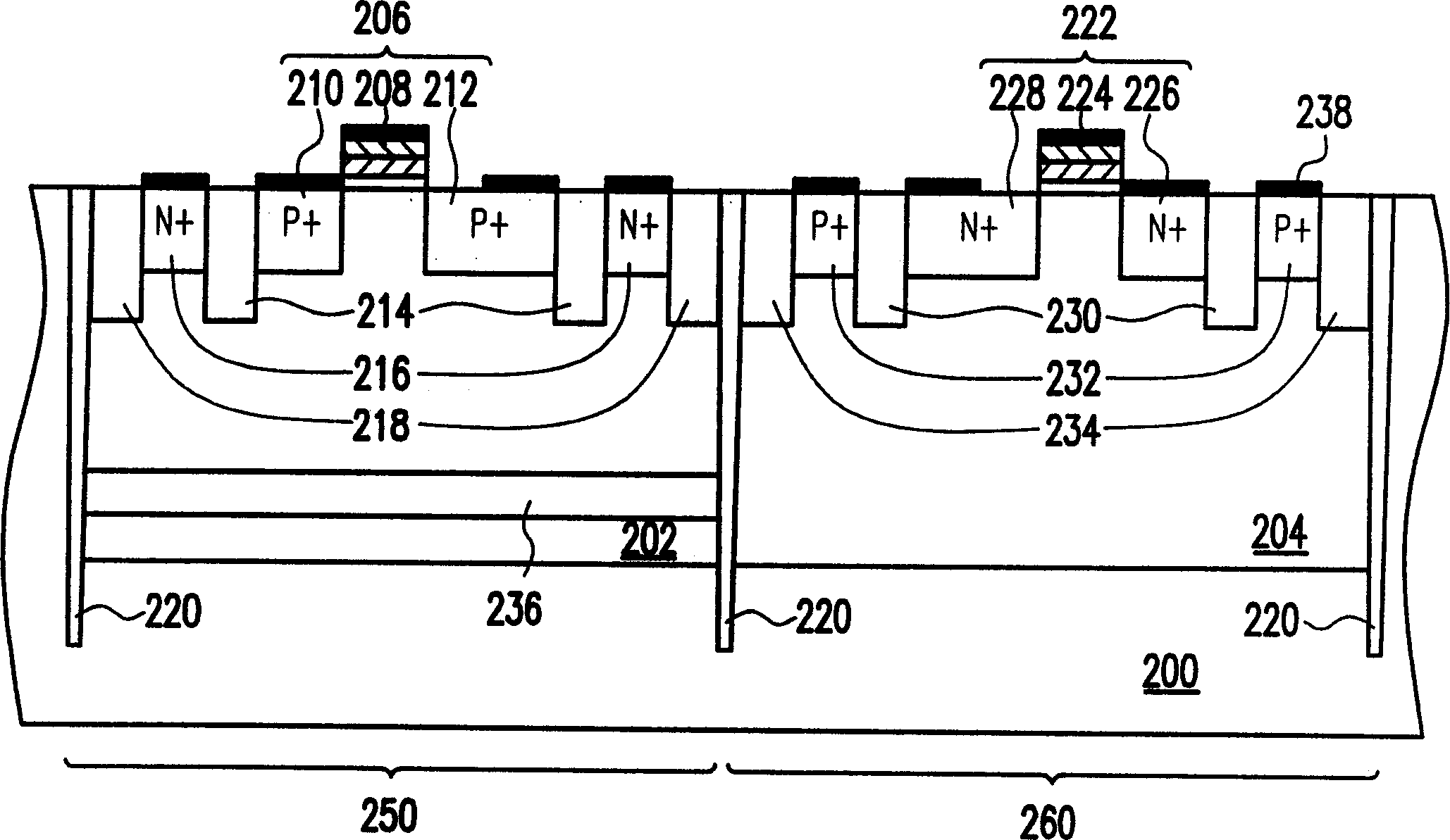
[0052] figure 2 It is a structural schematic diagram of the electrostatic discharge protection circuit of the present invention.

[0053] Please refer to figure 2 ,exist figure 2 In the PMOS region 250 of the P-type substrate 200, an N-well region 202 is provided, wherein the depth of the N-well region 202 is, for example, about 2 μm. Then, a PMOS transistor 206 and an N+ pedestal connection region 216 are disposed in the N well region 202 . The PMOS transistor 206 is composed of a gate 208 , a source 210 and a drain 212 . And in the N well region 202 , the N+ pedestal connection region 216 and the PMOS transistor 206 are separated by the shallow trench isolation layer 214 . In a preferred embodiment of the present invention, the depth of the shallow trench isolation layer 214 is, for example, about 4000 angstroms.

[0054] Moreover, a deep trench isolation layer 220 is provided outside the N+ base connection region 216 to replace the known guard ring. As far as the PM...


PUM

PropertyMeasurementUnit
Depthaaaaaaaaaa

Abstract

A deep trench is used in a circuit of electrostatic discharge protection to replace a guard ring circumjacent the electrostatic discharge protection circuit. The invention utilizes a fewer component area than the area utilized by the guard ring as well as shortens the distances between the transisters in the electrostatic discharge protection circuit to save the space and provide favorable functions of locking prevntion and noice provention.

Description

technical field [0001] The present invention relates to a structure and a manufacturing method of an electrostatic discharge protection circuit, and in particular to a structure and a manufacturing method of an electrostatic discharge protection circuit using a deep trench (Deep Trench) instead of a guard ring. Background technique [0002] Electrostatic discharge is the phenomenon of movement of static electricity from non-conductive surfaces that can cause damage to semiconductors and other circuit components in an IC. For example, a human body walking on a carpet can detect a static voltage of several hundred to several thousand volts when the relative humidity (RH) is high, and a static voltage of about several thousand volts can be detected when the relative humidity is low. Static voltage above 10,000 volts. A static voltage of several hundred to several thousand volts may also be generated in a machine for packaging integrated circuits or an instrument for testing in...

Claims


Application Information

Patent Timeline
IPC IPC(8): H01L21/336H01L21/70H01L23/60H01L27/02H01L27/092H01L29/78
CPCH01L27/0251
Inventor 陈孝贤许村来唐天浩曾华洲
Owner UNITED MICROELECTRONICS CORP
Why Eureka
Try Eureka